Planar silicon carbide reverse-blocking MOSFET device and preparation method thereof

A silicon carbide, planar technology, applied in semiconductor/solid-state device manufacturing, semiconductor devices, electrical components, etc., to achieve the effects of large forward and reverse symmetrical withstand voltage, reduced leakage current, and large forward withstand voltage

Active Publication Date: 2021-04-20
UNIV OF ELECTRONICS SCI & TECH OF CHINA
View PDF5 Cites 4 Cited by
  • Summary
  • Abstract
  • Description
  • Claims
  • Application Information

AI Technical Summary

Problems solved by technology

[0005] The purpose of the present invention is to solve the problem of how to make the planar silicon carbide MOSFET have a large positive and negative symmetrical withstand voltage and how to reduce its conduction voltage drop

Method used


Image

  • Planar silicon carbide reverse-blocking MOSFET device and preparation method thereof
  • Planar silicon carbide reverse-blocking MOSFET device and preparation method thereof
  • Planar silicon carbide reverse-blocking MOSFET device and preparation method thereof

Examples


Embodiment 1

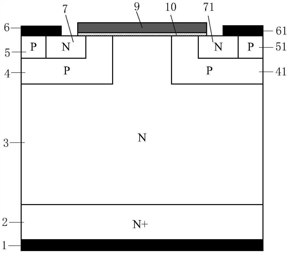
[0077] A reverse-resistance silicon carbide MOSFET, its cell structure is as follows figure 2 As shown, it includes: a back drain metal 1, a second N-type silicon carbide buffer layer 21, an N-type silicon carbide epitaxial layer 3, and a first N-type silicon carbide buffer layer 11 stacked in sequence from bottom to top; The N-type silicon carbide buffer layer 11 has a first P-type silicon carbide base region 4 and a second P-type silicon carbide base region 41; the lower part of the first N-type silicon carbide buffer layer 11 is in contact with the N-type silicon carbide epitaxial layer 3 , the upper part of the first N-type silicon carbide buffer layer 11 separates the first P-type silicon carbide base region 4 and the second P-type silicon carbide base region 41; the first P-type silicon carbide base region 4 has a second A P-type silicon carbide source region 5 and a first N-type silicon carbide source region 7; the first P-type silicon carbide source region 5 is in con...

Embodiment 2

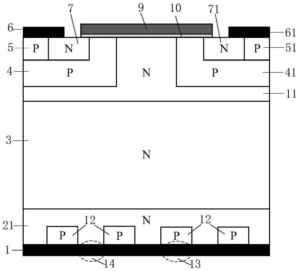
[0093] A reverse-resistance silicon carbide MOSFET, its cell structure is as follows image 3 As shown, the difference between this embodiment and Embodiment 1 is that: the second N-type silicon carbide buffer layer 21 has a P-type floating region 17 that is not connected; There is no contact between them, completely floating in the second N-type silicon carbide buffer layer 21 ; a Schottky contact is formed between the second N-type silicon carbide buffer layer 21 and the back drain metal 1 .

[0094] Preferably, all silicon carbide materials are replaced with gallium nitride, gallium oxide, boron nitride, and silicon materials.

[0095] This embodiment also provides a method for preparing a planar silicon carbide reverse resistance MOSFET device, including the following preparation steps:

[0096] Step 1: using an epitaxial process to prepare a second N-type silicon carbide buffer layer 21 on the surface of the N-type silicon carbide substrate 2;

[0097] Step 2: using an ...

Embodiment 3

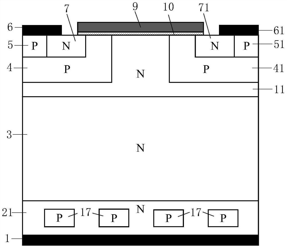
[0108] A kind of derivation structure of embodiment 1, its cell structure is as Figure 4 shown. In this embodiment, the N-type silicon carbide epitaxial layer 3 in Embodiment 1 is replaced by P pillars 31 and N pillars 32 , and other structures are the same as those in Embodiment 1.

[0109] In this embodiment, a super junction MOSFET structure is formed by introducing P pillars 31 and N pillars 32 . The specific principle is: when the P column 31 and the N column 32 reach the charge balance, the external non-electricity of the entire drift region can be approximately neutral, which makes the concentration and withstand voltage of the drift region relatively independent. This embodiment can ensure that the conduction voltage drop of the device is effectively reduced under the same withstand voltage level, and the performance of the device is improved.


PUM


Abstract

The invention belongs to the technical field of power semiconductor devices, and particularly relates to a planar silicon carbide reverse-blocking MOSFET device and a preparation method thereof. Compared with a traditional planar silicon carbide MOSFET, the planar silicon carbide reverse-blocking MOSFET device in the invention has the following advantages: an N-type silicon carbide substrate is removed, a first N-type silicon carbide buffer layer is introduced to one side of a source region of the device, a second N-type silicon carbide buffer layer is introduced to one side of a drain region of the device, and a junction Schottky barrier diode structure is introduced to one side of the drain region of the device. According to the above device structure, planar silicon carbide MOSFET has relatively small forward conduction voltage drop while obtaining large forward and reverse symmetrical withstand voltage. In addition, in order to further improve the withstand voltage and conduction characteristics of the device, several corresponding derivative structures are provided.

Description

technical field [0001] The invention belongs to the technical field of power semiconductor devices, and in particular relates to a planar silicon carbide reverse resistance MOSFET device and a preparation method thereof. Background technique [0002] The inverter is a device that converts direct current into alternating current. It has a wide range of application scenarios, such as photovoltaic inverters, uninterruptible power supplies, rail transit and trolleybuses, and frequency converters. Multilevel inverters have excellent characteristics such as low loss, low noise, and output waveforms close to sine waves, so their application scenarios are broader. Matrix inverter is a new type of power converter, which can directly realize AC-AC conversion. Compared with the traditional AC-DC-AC frequency conversion method, the matrix inverter does not require DC capacitors for intermediate energy storage, which improves the reliability of the entire system and reduces costs. [0...

Claims


Application Information

Patent Timeline
Patent Type & Authority Applications(China)
IPC IPC(8): H01L29/78H01L29/47H01L29/45H01L29/06H01L21/336
Inventor 张金平王鹏蛟陈伟刘竞秀张波
Owner UNIV OF ELECTRONICS SCI & TECH OF CHINA
Why Eureka
Try Eureka