Lateral trench insulated gate bipolar translator (IGBT) having self-biased positive channel metal oxide semiconductor (PMOS) and its preparation method

A lateral groove and self-bias technology, which is applied in semiconductor/solid-state device manufacturing, semiconductor devices, electrical components, etc., can solve the problems of reducing conduction voltage drop, slow turn-off speed, large turn-off loss, etc., and achieves reduction On-voltage drop, increased blocking voltage, and easy-to-drive effects

Active Publication Date: 2019-11-26
UNIV OF ELECTRONIC SCI & TECH OF CHINA
View PDF11 Cites 4 Cited by
  • Summary
  • Abstract
  • Description
  • Claims
  • Application Information

AI Technical Summary

Problems solved by technology

When the device is forward-blocked, the base region of the drift region is depleted each other, and its depletion layer bears a high withstand voltage, while the silicon dioxide buried layer of SOI assists the withstand voltage; when the device is forward-conducted, the parasitic pnp transistor is turned on, and at the same time The base current is injected into the pnp transistor through the MOS channel, so that the p

Method used


Image

  • Lateral trench insulated gate bipolar translator (IGBT) having self-biased positive channel metal oxide semiconductor (PMOS) and its preparation method
  • Lateral trench insulated gate bipolar translator (IGBT) having self-biased positive channel metal oxide semiconductor (PMOS) and its preparation method
  • Lateral trench insulated gate bipolar translator (IGBT) having self-biased positive channel metal oxide semiconductor (PMOS) and its preparation method

Examples


Embodiment 1

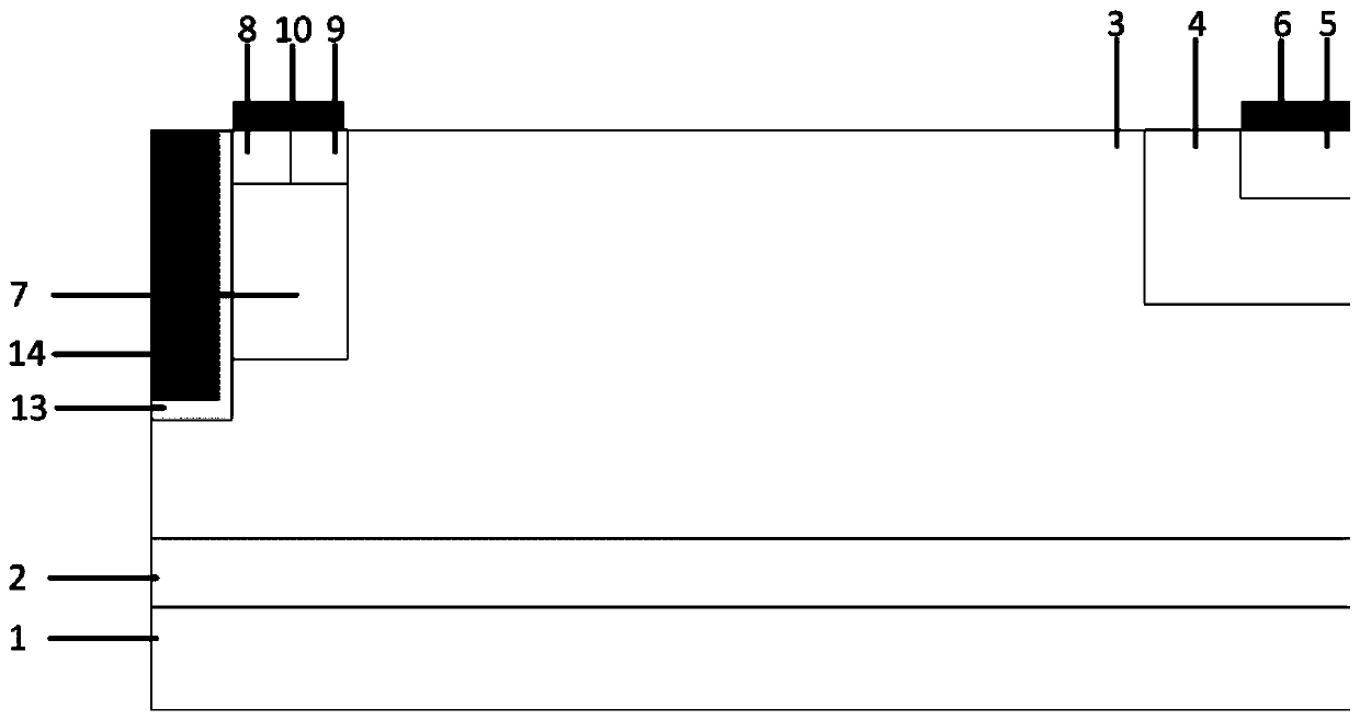
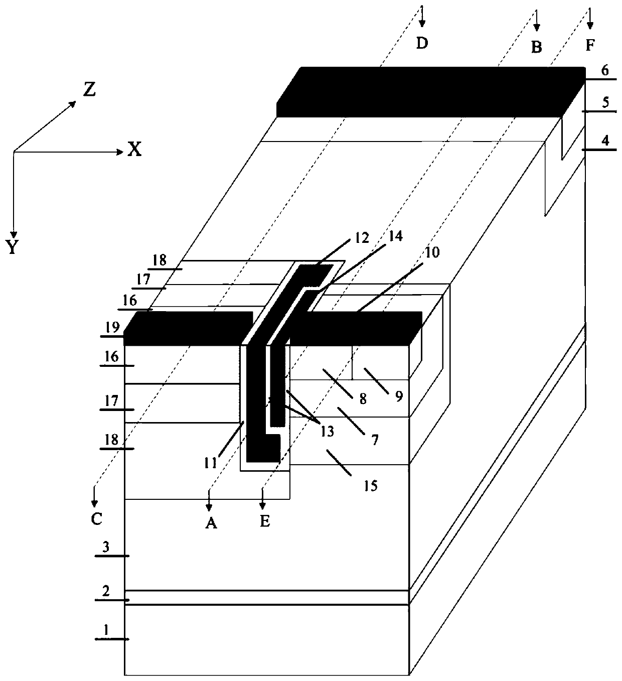
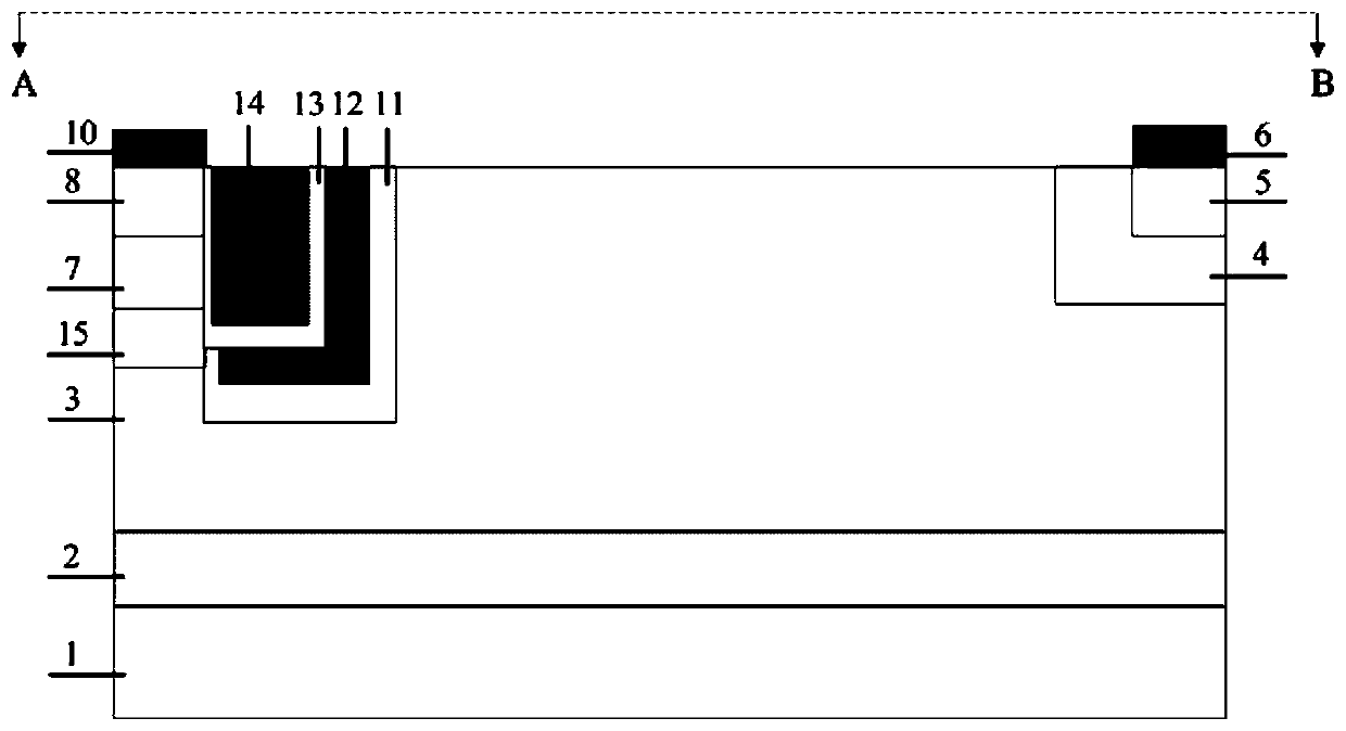
[0062] This embodiment provides a lateral insulated gate bipolar transistor whose half-cell structure is as follows figure 2 As shown, the two-dimensional cross-sectional structures obtained along the dotted line AB and dotted line CD in the semi-cellular structure are as follows image 3 and Figure 4shown. This embodiment includes a P-type substrate 1, a silicon dioxide isolation layer 2, and an N-type drift region 3 arranged in sequence from bottom to top; an N-type buffer zone 4 is arranged on one side of the top layer of the N-type drift region 3 in the longitudinal direction, so The longitudinal direction is the third dimension perpendicular to the horizontal and vertical directions of the device; the N-type buffer zone 4 is provided with an N-type collector region 5, and the upper surface of the N-type collector region 5 is provided with a first metallized collector 6; in the N-type drift region 3, the top of the side away from the N-type buffer zone 4 in the longitu...

Embodiment 2

[0071] This embodiment provides a lateral insulated gate bipolar transistor, the half-cell structure of which is as follows Figure 5 shown. In this embodiment, on the basis of Embodiment 1, a third gate oxide layer 131 is provided on the upper surface of the P-type base region 8, and the third gate oxide layer 131 extends vertically above the N-type charge storage region 15; the third gate oxide layer A second polysilicon gate electrode 141 is disposed over layer 131 .

[0072] In particular, the horizontal direction of the third gate oxide layer 131 and the second polysilicon gate electrode 141 may be in contact with the border of the right half cell or the border of the N-type emitter region 8 .

[0073] In particular, a surface channel may be formed on the surface of the device under the second polysilicon gate electrode 141 when the device is turned on.

[0074] Compared with Embodiment 1, due to the existence of the third gate oxide layer 131 and the second polysilicon...

Embodiment 3

[0076] This embodiment provides a lateral insulated gate bipolar transistor, the half-cell structure of which is as follows Image 6 shown. In this embodiment, on the basis of Embodiment 1, the second trench structure includes a first polysilicon gate electrode 14 and a second silicon dioxide layer disposed on the side wall and bottom wall of the first polysilicon gate electrode 14 13 is transferred to the longitudinal direction of the N-type emitter region 8 and the P-type emitter region 9, and the second silicon dioxide layer 13 is in contact with the N-type emitter region 8 and the P-type emitter region 9; the position of the original second trench structure is determined by the second The second polysilicon emitter 12 is filled with the first silicon dioxide layer 11 disposed on the side wall and the bottom wall of the second polysilicon emitter 12 .


PUM

PropertyMeasurementUnit
Thicknessaaaaaaaaaa

Abstract

The invention belongs to the technical field of power semiconductor devices and relates to a lateral trench insulated gate bipolar translator (IGBT) having a positive channel metal oxide semiconductor(PMOS) and its preparation method. Based on a lateral IGBT (LIGBT) device structure, a current carrier storage layer is added to the lateral-trench IGBT having the self-biased PMOS to enhance the conductivity modulation effect, and reduce the device conduction pressure drop; a side face of a grid electrode is wrapped by a sorting grid to reduce the Miller capacitance, reduce the turn-off time, reduce the turn-off loss, and improve the compromise between the forward conduction voltage drop and the turn-off loss; in the meanwhile, the gate charge of a device can be reduced, and drive loss is reduced; the compromise characteristic between a current decline rate (di/dt) and the conduction loss (Eon) is improved; automatic turn-on of a metal-oxide-semiconductor field-effect transistor (MOSFET)is self-biased during forward conduction, a voltage of a charge storage area is clamped, a saturation current is reduced and a short-circuit safe working area is optimized; the turn-on of the MOSFETself-biased in a preliminary stage is turned off, extraction of remaining current carriers of a drift region is accelerated, and the turn-off loss is reduced; a buried layer on a left side of trench gate can assist voltage resistance, and a blocking voltage is increased; and a thin gate oxide layer can reduce a threshold voltage of the device, and reduce the current densify of a latch.

Description

technical field [0001] The invention belongs to the technical field of power semiconductors, and in particular relates to a lateral trench type insulated gate bipolar transistor. Background technique [0002] Insulated gate bipolar transistor (IGBT) is a widely used power electronic device, which has the characteristics of high input impedance, simple driving circuit, high current density and low saturation voltage. The lateral IGBT device is a horizontally integrated power device developed on the basis of the IGBT. It combines the advantages of the IGBT device structure, such as high input impedance, low driving power, reduced conduction voltage, fast switching speed, and strong voltage blocking capability. , and has gained important applications in the field of horizontally integrated devices. [0003] With the continuous improvement of the integration level of lateral semiconductor devices and the continuous reduction of feature size, the interaction between closely arra...

Claims


Application Information

Patent Timeline
IPC IPC(8): H01L27/07H01L29/06H01L21/84
CPCH01L27/0705H01L21/84H01L29/0603H01L29/0684
Inventor 张金平赵阳罗君轶刘竞秀李泽宏张波
Owner UNIV OF ELECTRONIC SCI & TECH OF CHINA
Why Eureka
Try Eureka