Semiconductor device

A technology of semiconductor and barrier layer, applied in the field of semiconductor devices with diode structure, can solve the problem of reducing the effect of suppressing hole injection and the like

Active Publication Date: 2021-09-24
DENSO CORP
View PDF9 Cites 0 Cited by
  • Summary
  • Abstract
  • Description
  • Claims
  • Application Information

AI Technical Summary

Problems solved by technology

However, if the carrier density in the barrier region is reduced, the aforementioned effect of suppressing hole injection will be reduced.

Method used


Image

  • Semiconductor device
  • Semiconductor device
  • Semiconductor device

Examples


Embodiment Construction

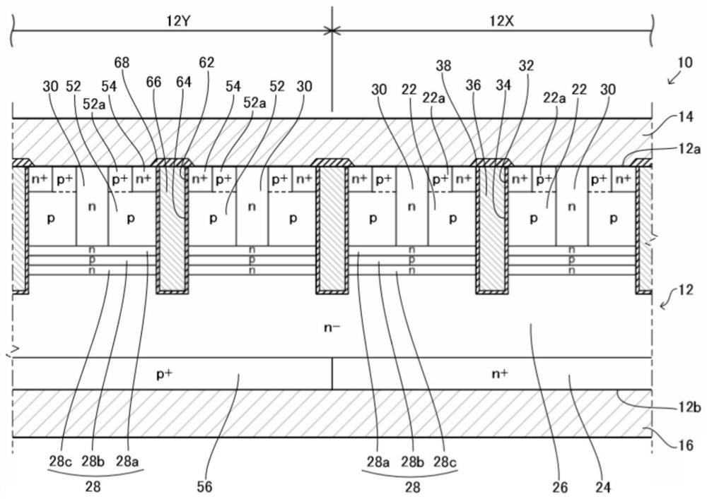
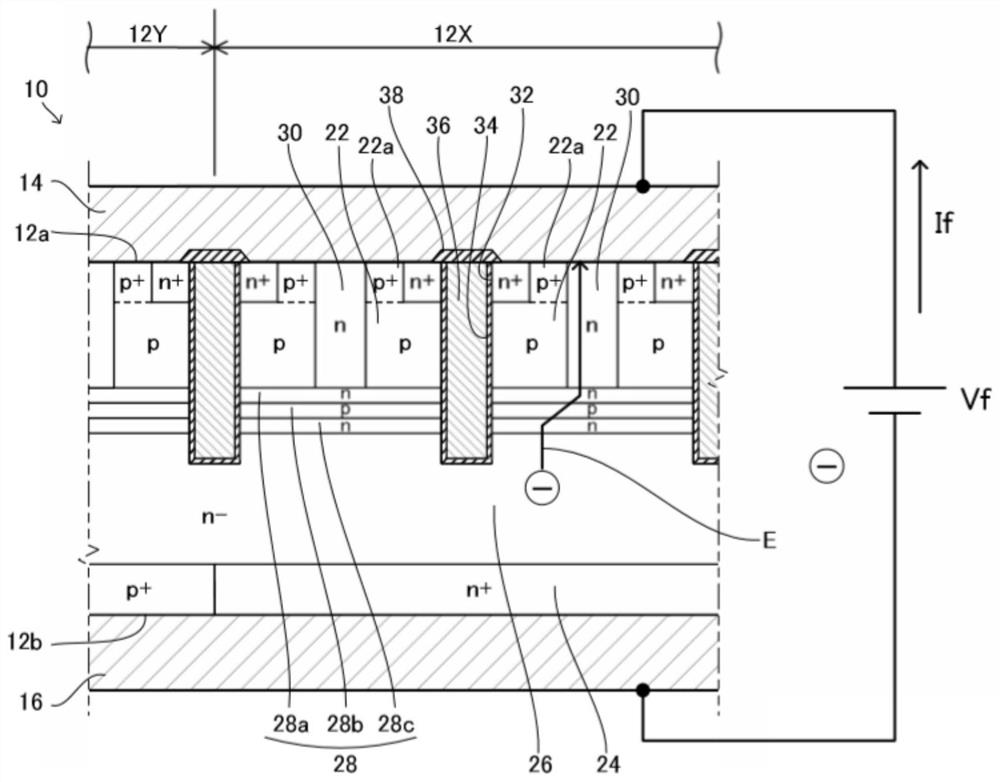
[0017] In one embodiment of the present technology, when the semiconductor substrate has the aforementioned IGBT structure, the barrier region may further have a p-type fourth barrier layer between the third barrier layer and the drift layer. According to this structure, the area where the gate electrode faces the drift region via the gate insulating film can be reduced. Thereby, since the parasitic capacitance between the gate and the lower surface electrode is reduced, the IGBT can be turned off (ie, discharged from the gate) in a short time.

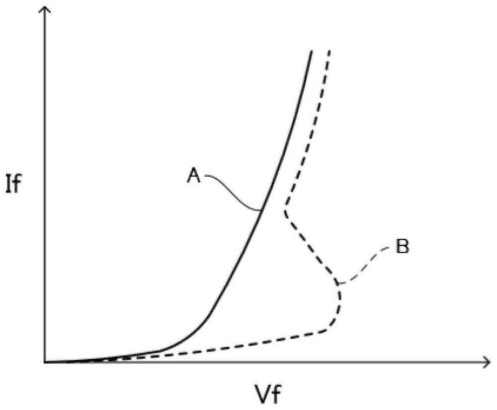
[0018] In one embodiment of the present technology, the carrier density of the third barrier layer may be higher than that of the first barrier layer. According to this structure, when the semiconductor device functions as a diode, the recovery current can be reduced while suppressing the occurrence of the hysteresis phenomenon. In addition, when the semiconductor device functions as an IGBT, the conductance modulation of the drift r...


PUM


Abstract

The present invention provides a semiconductor device having a semiconductor substrate, an upper surface electrode, and a lower surface electrode. The semiconductor substrate has: a p-type anode region in contact with the upper surface electrode, an n-type cathode region in contact with the lower surface electrode, and a drift region between the anode region and the cathode region. The semiconductor substrate also has a barrier region located between the anode region and the drift region, and an n-type pillar region extending between the barrier region and the upper surface electrode. The potential barrier region has a multilayer structure, the multilayer structure includes an n-type first potential barrier layer, a p-type second potential barrier layer, and an n-type third potential barrier layer, and the second potential barrier layer is located at the first potential barrier layer. between the barrier layer and the third barrier layer. The first potential barrier layer is in contact with the anode region, and is connected to the upper surface electrode through the column region.

Description

technical field [0001] The technology disclosed in this specification relates to a semiconductor device, and more particularly, to a semiconductor device having a diode structure. Background technique [0002] Japanese Patent Laid-Open No. 2016-162897 discloses a semiconductor device having a diode structure. The semiconductor device has a semiconductor substrate, an upper surface electrode provided on an upper surface of the semiconductor substrate, and a lower surface electrode provided on a lower surface of the semiconductor substrate on the opposite side of the upper surface. The semiconductor substrate has a p-type anode region in contact with the upper surface electrode, an n-type cathode region in contact with the lower surface electrode, and an n-type drift region located between the anode region and the cathode region and having a lower carrier density than the cathode region. [0003] The semiconductor device also has an n-type barrier region between the anode reg...

Claims


Application Information

Patent Timeline
Patent Type & Authority Patents(China)
IPC IPC(8): H01L29/739H01L29/06
CPCH01L29/0684H01L29/7397H01L27/0727H01L29/407H01L29/0834H01L29/1095H01L29/1608H01L29/0603H01L29/861H01L27/0716H01L29/083H01L29/41708H01L29/0804H01L29/0821H01L29/4236
Inventor 平林康弘
Owner DENSO CORP
Why Eureka
Try Eureka