Power and ground routing of integrated circuit devices with improved ir drop and chip performance

a technology of integrated circuits and chip devices, which is applied in the direction of semiconductor devices, semiconductor/solid-state device details, electrical apparatus, etc., can solve the problems of unavoidable voltage drop (or ir drop), and achieve the effect of improving chip performance, power and ground routing, and reducing ir drop

Active Publication Date: 2012-02-23
MEDIATEK INC
View PDF2 Cites 20 Cited by
  • Summary
  • Abstract
  • Description
  • Claims
  • Application Information

AI Technical Summary

Benefits of technology

[0014]It is one object of the invention to provide an improved power and ground routing for the integrated circuit chip devices that is capable of reducing the IR drop and improving the chip performance.
[0015]It is another object of the invention to provide an integrated circuit chip device that utilizes aluminum layer over passivation to form power or ground lines, thereby reducing the IR drop of the integrated circuit chip device and improving the performance thereof.

Problems solved by technology

This is due to technological processing constraints such as smaller thickness at the lower layers.
The prior art approach of using the topmost two levels of the copper metal layers, i.e., M5 and M6, for power and ground routing induces that the voltage drop (or IR drop) is unavoidably high.

Method used


Image

  • Power and ground routing of integrated circuit devices with improved ir drop and chip performance
  • Power and ground routing of integrated circuit devices with improved ir drop and chip performance
  • Power and ground routing of integrated circuit devices with improved ir drop and chip performance

Examples


Embodiment Construction

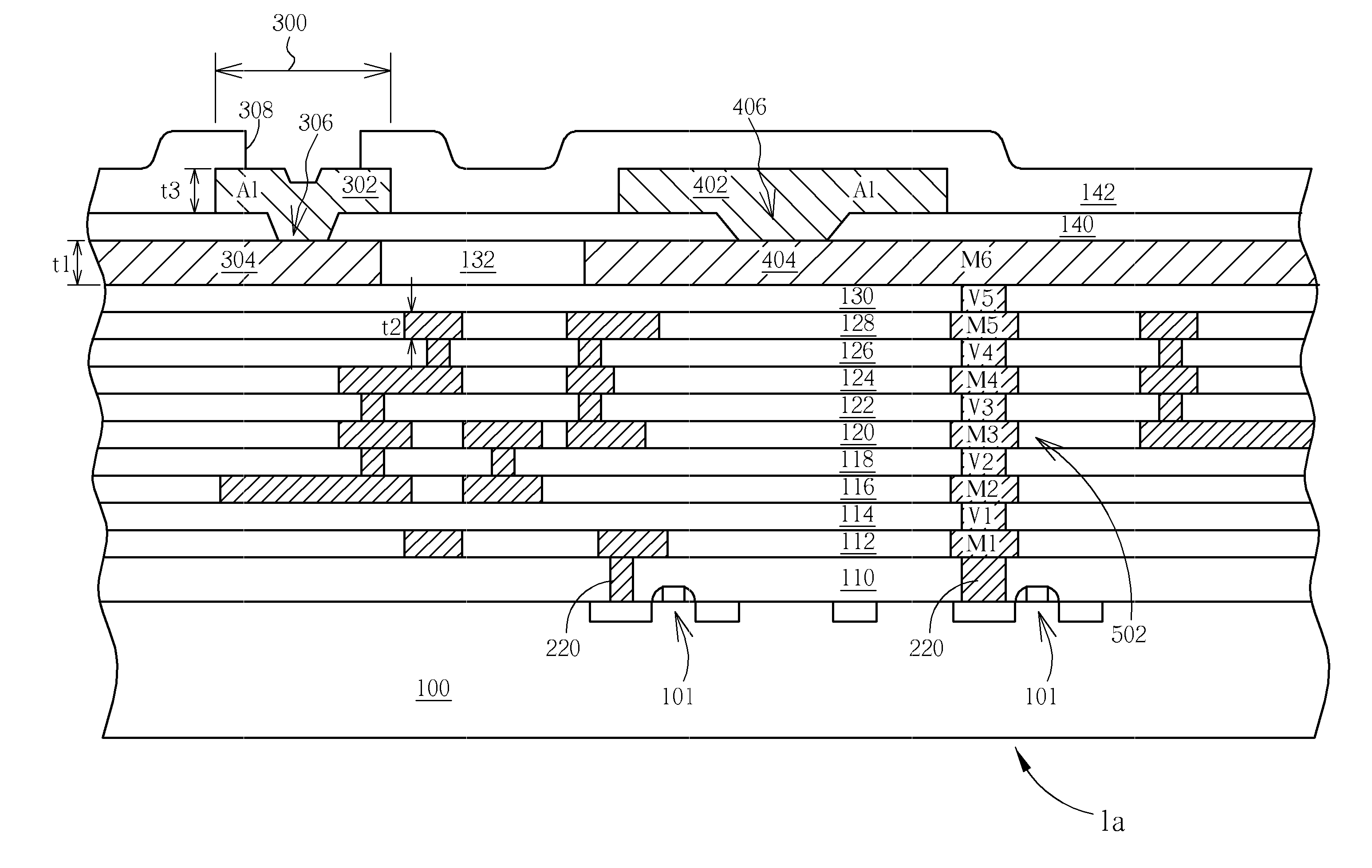
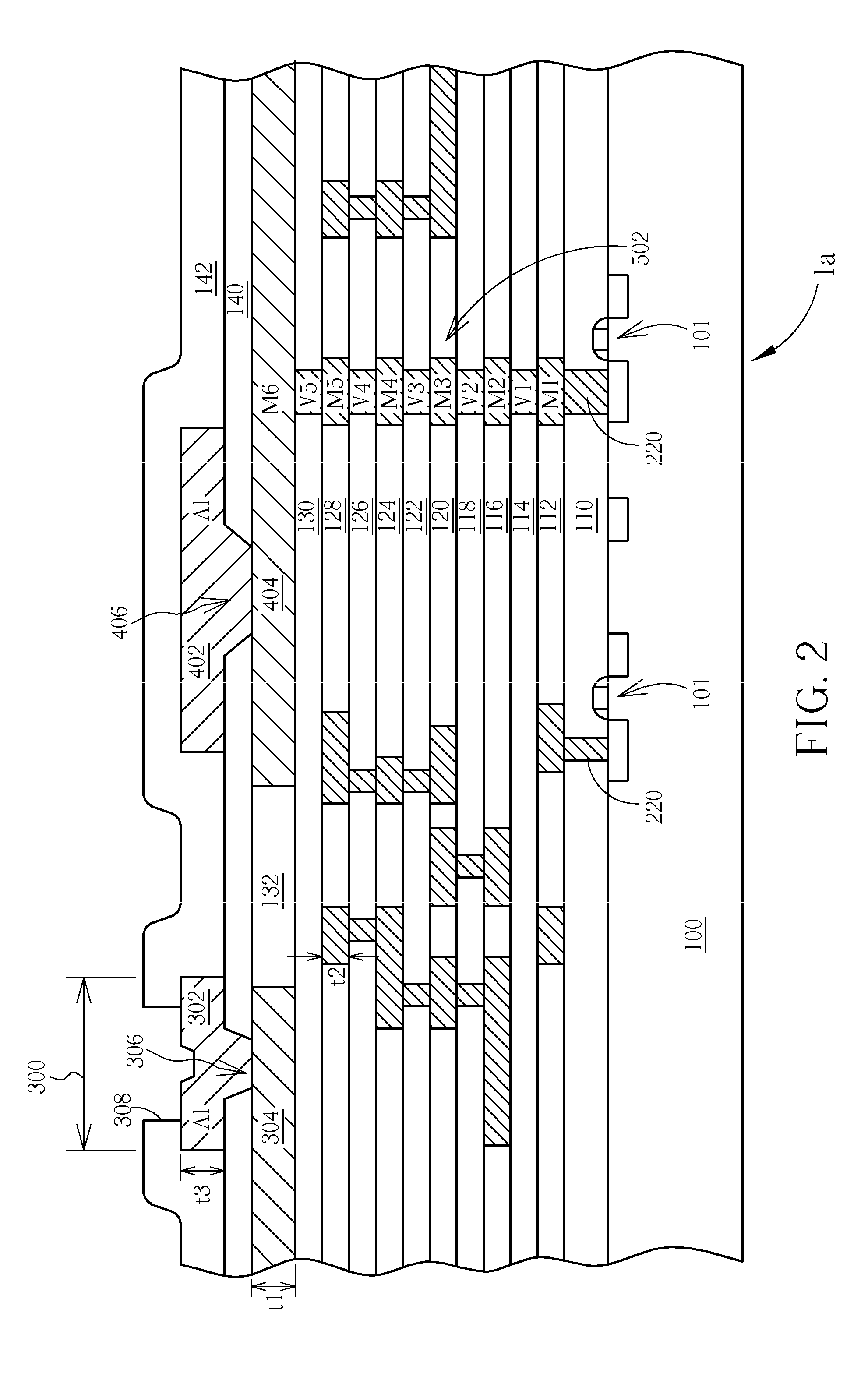
[0027]The invention pertains to a novel power and ground routing capable of improving the performance of the integrated circuit chip. The invention utilizes a layer of aluminum in a passivation layer of the integrated circuit chip to form the power or ground ring and / or mesh interconnection network instead of the copper metal layer (Mn−1) that is just one level lower than the topmost copper metal layer (Mn) of the integrated circuit chip. Therefore, one of the topmost two levels of the copper metal layers that used to be formed into power and ground rings and mesh interconnection network can thus be eliminated or be spared for signal routing. Alternatively, the replaced Mn−1 copper layer can be skipped for saving photomask and cost. The invention can increase signal routing source and increase the flexibility of placement and routing.

[0028]The preferred embodiments of this invention will now be explained with the accompanying figures. Throughout the specification and drawings, the s...


PUM


Abstract

An integrated circuit chip includes a semiconductor substrate having thereon a plurality of IMD layers and a plurality of first conductive layers; a first passivation layer overlying the plurality of IMD layers and the first conductive layers; at least a first power / ground mesh wiring line in a first aluminum layer overlying the first Insulating layer; and at least a second power / ground mesh wiring line in a second aluminum layer overlying the first aluminum layer.

Description

CROSS REFERENCE TO RELATED APPLICATIONS[0001]This is a continuation-in-part of U.S. patent application Ser. No. 12 / 883,163 filed Sep. 15, 2010, which itself is a continuation application of U.S. patent application Ser. No. 12 / 052,735 filed Mar. 21, 2008, now U.S. Pat. No. 7,821,038.BACKGROUND OF THE INVENTION[0002]1. Field of the Invention[0003]The invention relates generally to the integrated circuit power and ground routing and, more particularly, to a novel power and ground routing of integrated circuit (IC) chip devices that utilizes aluminum layer to form power or ground lines for distributing power across the IC from an off chip source to various blocks within the IC, thereby reducing the IR drop (or voltage drop) of the integrated circuit chip devices and improving the chip performance.[0004]2. Description of the Prior Art[0005]In the processes for designing a large-scale integrated semiconductor circuit device, respective blocks of the device are generally designed in parall...

Claims


Application Information

Patent Timeline
Patent Type & Authority Applications(United States)
IPC IPC(8): H01L23/52
CPCH01L21/823475H01L23/5286H01L2924/0002H01L2924/00H01L23/5226H01L23/53228H01L23/585H01L24/05H01L2224/05124H01L2924/14
Inventor KO, CHING-CHUNGCHENG, TAOLIU, TIEN-YUEHCHOU, TA-HSIKAO, PENG-CHENGKE, LING-WEI
Owner MEDIATEK INC
Why Eureka
Try Eureka