
Bipolar resistive-switching memory with a single diode per memory cell

a resistive switching and memory technology, applied in the field of semiconductor memories, can solve the problems of flash memory proving inadequate for non-volatile memory needs, and achieve the effect of reducing the number of diodes

Active Publication Date: 2012-02-23
INTERMOLECULAR
View PDF3 Cites 56 Cited by
  • Summary
  • Abstract
  • Description
  • Claims
  • Application Information

AI Technical Summary

Benefits of technology

"The patent describes a new type of memory called bipolar resistive-switching memory that uses a single diode as a select element, which is simpler and more efficient than previous designs. The memory elements switch using a transient-type switching mechanism with a short voltage pulse, and the switch speed is faster than previous non-volatile memories like flash memory. The technical effect of this invention is to provide a more efficient and faster non-volatile memory that can meet the requirements of current electronic devices."

Problems solved by technology

Flash memory is proving, in many instances, to be inadequate for non-volatile memory needs.

Method used


Image

  • Bipolar resistive-switching memory with a single diode per memory cell
  • Bipolar resistive-switching memory with a single diode per memory cell
  • Bipolar resistive-switching memory with a single diode per memory cell

Examples


Embodiment Construction

[0017]A detailed description of one or more embodiments is provided below along with accompanying figures. The detailed description is provided in connection with such embodiments, but is not limited to any particular example. The scope is limited only by the claims and numerous alternatives, modifications, and equivalents are encompassed. Numerous specific details are set forth in the following description in order to provide a thorough understanding. These details are provided for the purpose of example and the described techniques may be practiced according to the claims without some or all of these specific details. For the purpose of clarity, technical material that is known in the technical fields related to the embodiments has not been described in detail to avoid unnecessarily obscuring the description.

[0018]According to various embodiments, a resistive-switching memory element and memory element array that uses a bipolar switching includes a select element comprising only a...


PUM


Abstract

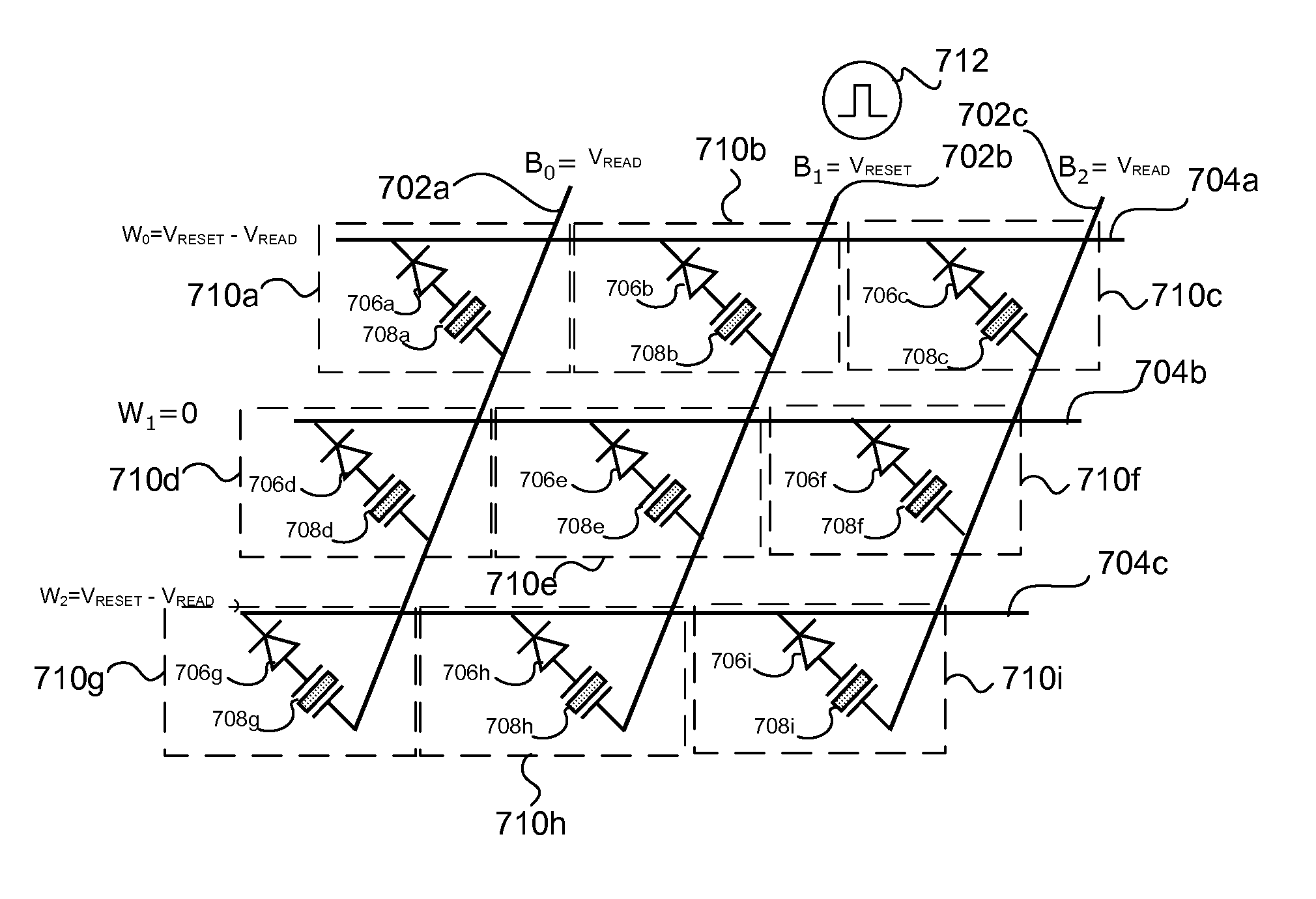
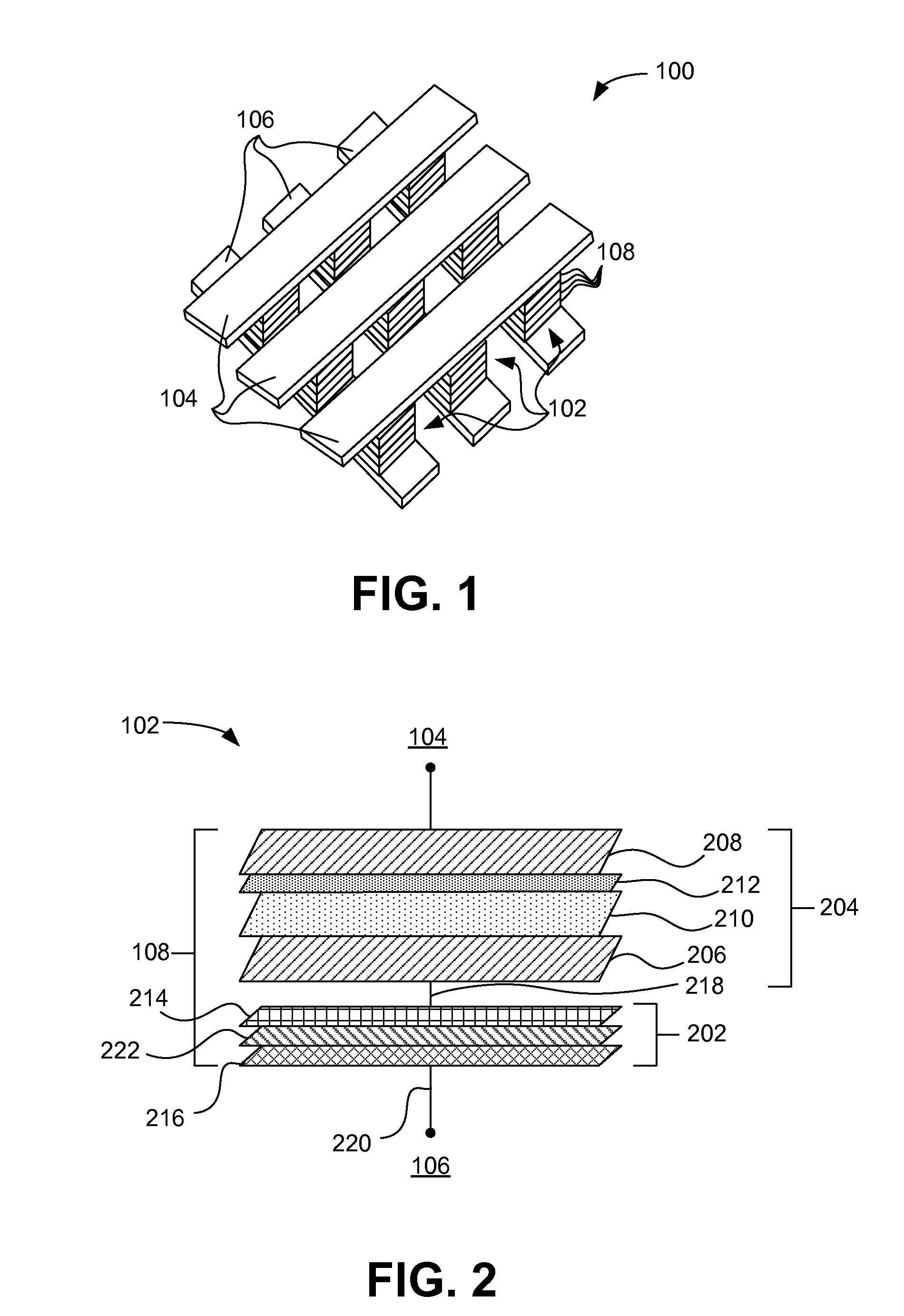
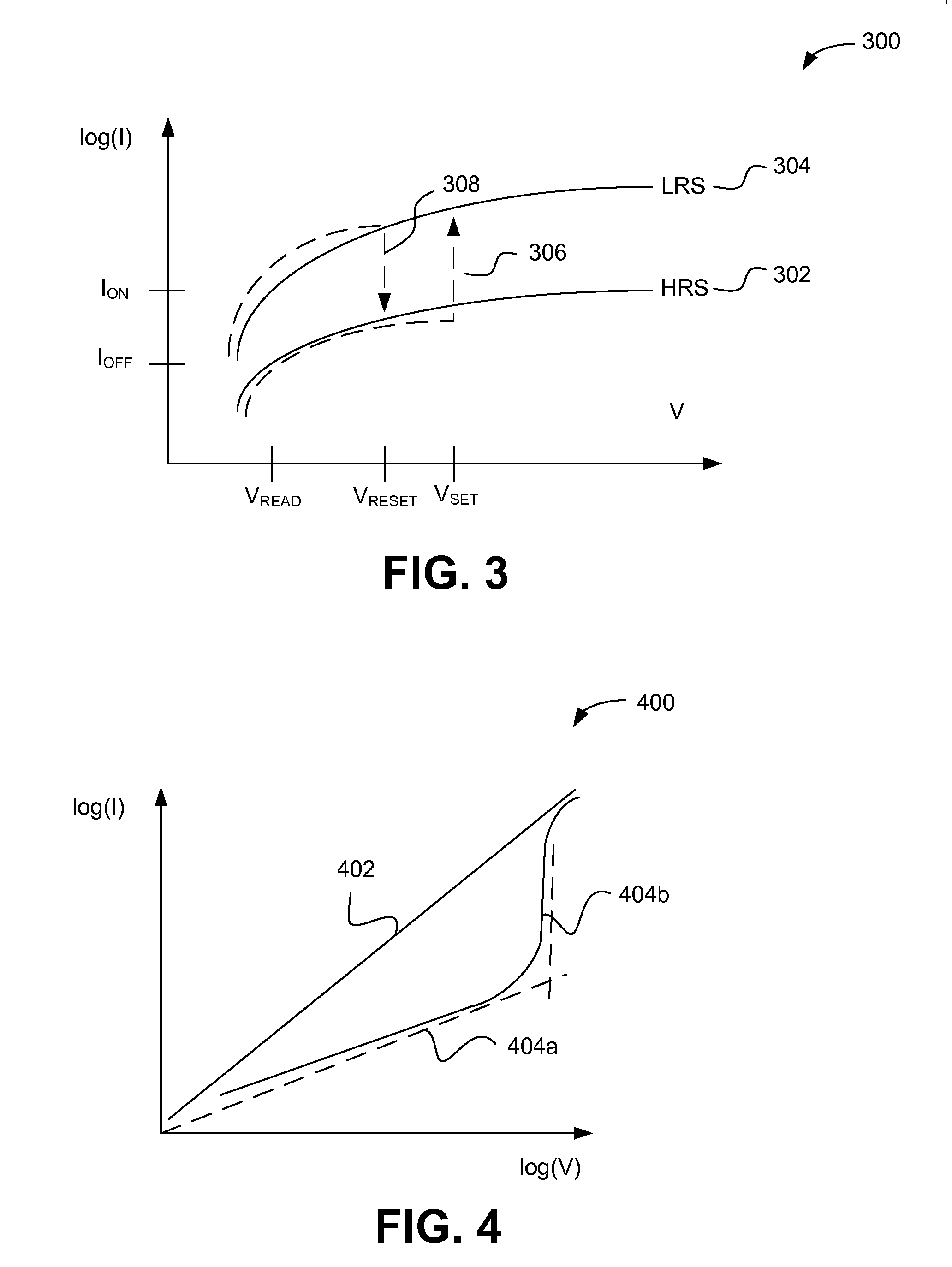
According to various embodiments, a resistive-switching memory element and memory element array that uses a bipolar switching includes a select element comprising only a single diode that is not a Zener diode. The resistive-switching memory elements described herein can switch even when a switching voltage less than the breakdown voltage of the diode is applied in the reverse-bias direction of the diode. The memory elements are able to switch during the very brief period when a transient pulse voltage is visible to the memory element, and therefore can use a single diode per memory cell.

Description

RELATED APPLICATIONS[0001]This application is a Divisional Application of U.S. application Ser. No. 12 / 607,898 entitled “Bipolar Resistive-Switching Memory With A Single Diode Per Memory Cell” and filed on Oct. 28, 2009 with a Notice of Allowance date of Oct. 25, 2011 which is incorporated herein by referenceFIELD OF THE INVENTION[0002]The present invention relates generally to semiconductor memories. More specifically, a bipolar resistive-switching memory with a single diode per memory cell is described.BACKGROUND OF THE INVENTION[0003]Non-volatile memories are semiconductor memories that retain their contents when unpowered. Non-volatile memories are used for storage in electronic devices such as digital cameras, cellular telephones, and music players, as well as in general computer systems, embedded systems and other electronic devices that require persistent storage. Non-volatile semiconductor memories can take the form of removable and portable memory cards or other memory modu...

Claims


Application Information

Patent Timeline
Patent Type & Authority Applications(United States)
IPC IPC(8): G11C11/36
CPCG11C13/0007G11C13/0069G11C2013/0073G11C2013/0092G11C2213/72G11C7/00G11C11/36G11C13/02G11C13/04G11C13/0002G11C13/0021
Inventor WANG, YUNPHATAK, PRASHANTCHIANG, TONY
Owner INTERMOLECULAR
Learn More