Display panel

a display panel and panel technology, applied in non-linear optics, instruments, optics, etc., can solve problems such as line defects, pixels malfunction, and broken lines, and achieve the effect of preventing an rc overloading effect and ensuring display quality after repair

Active Publication Date: 2012-03-01
AU OPTRONICS CORP
View PDF1 Cites 10 Cited by
  • Summary
  • Abstract
  • Description
  • Claims
  • Application Information

AI Technical Summary

Benefits of technology

[0009]The invention is directed to a display panel which can prevent an RC overloading effect on a repairing line, so as to ensure the display quality after repair.

Problems solved by technology

The great length of scan lines and data lines on the active device array substrate easily results in broken lines.
When a scan line or a data line is broken, some of the pixels malfunction, and a line defect occurs.
When the repairing line is connected to the broken signal line through the welding points, a RC overloading effect on the repairing line is likely to occur due to the excessive capacitance generated between the repairing line and the electrode layer.
As such, signal transmission on the signal line is negatively affected.
Namely, the RC overloading effect caused by the repairing operation results in distorted signals during transmission, thereby affecting the display quality of the display panel.

Method used


Image

  • Display panel
  • Display panel
  • Display panel

Examples


first embodiment

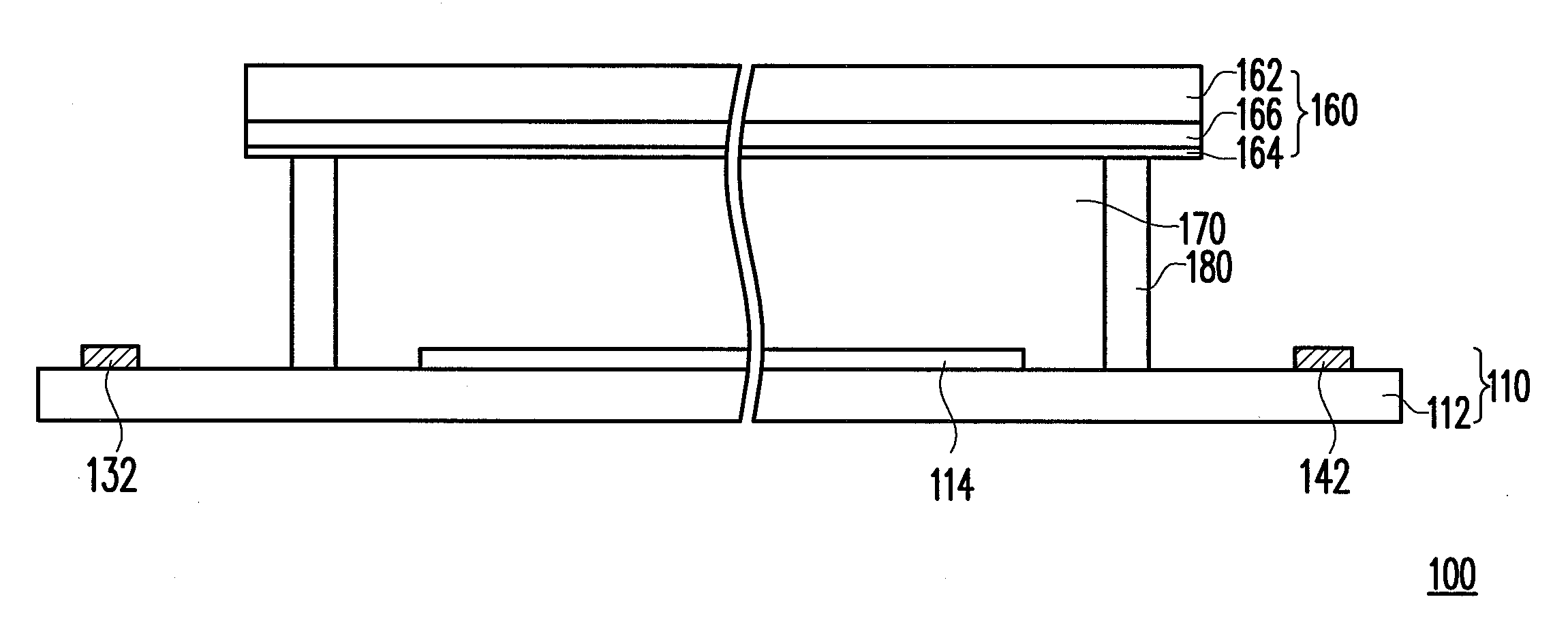
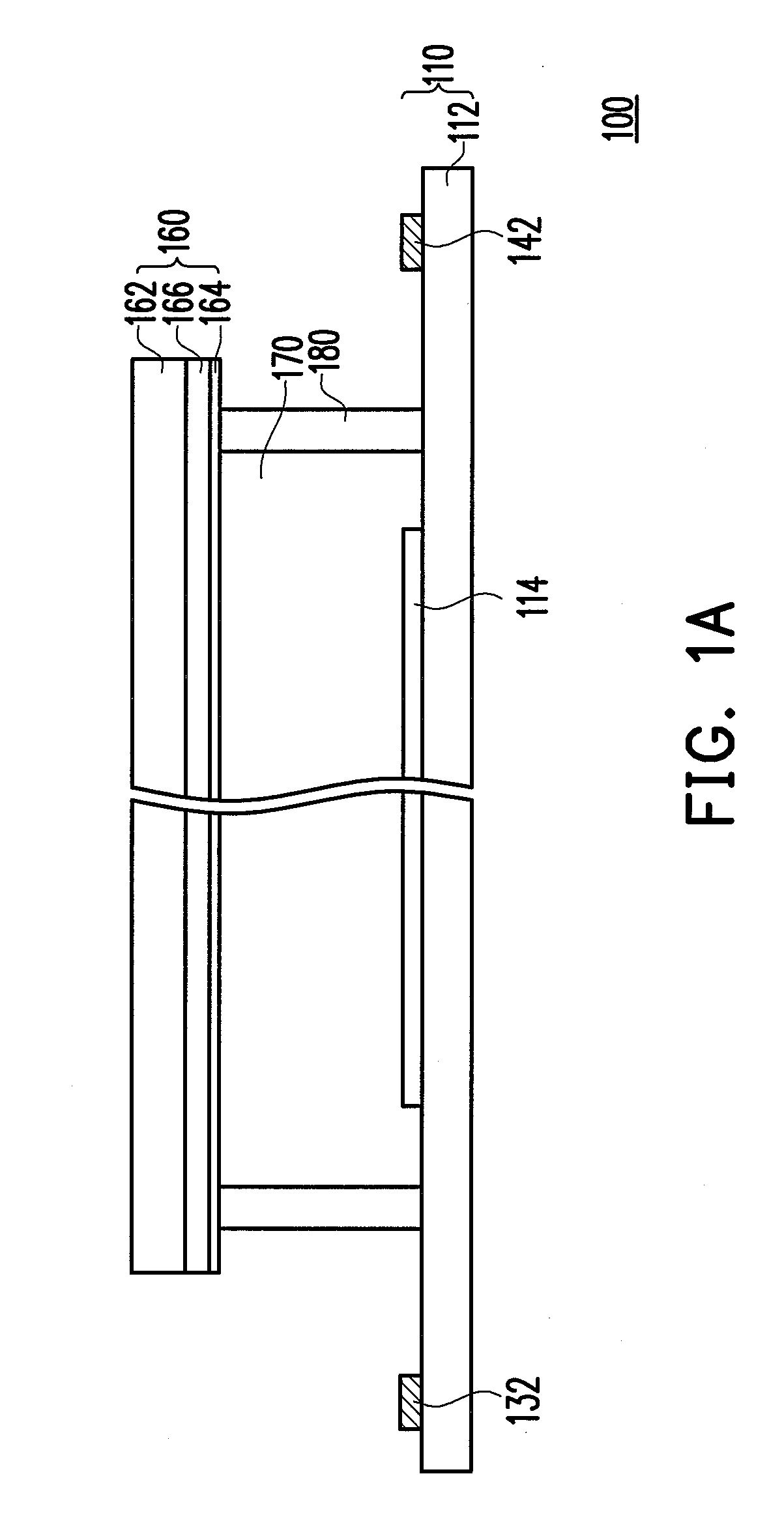
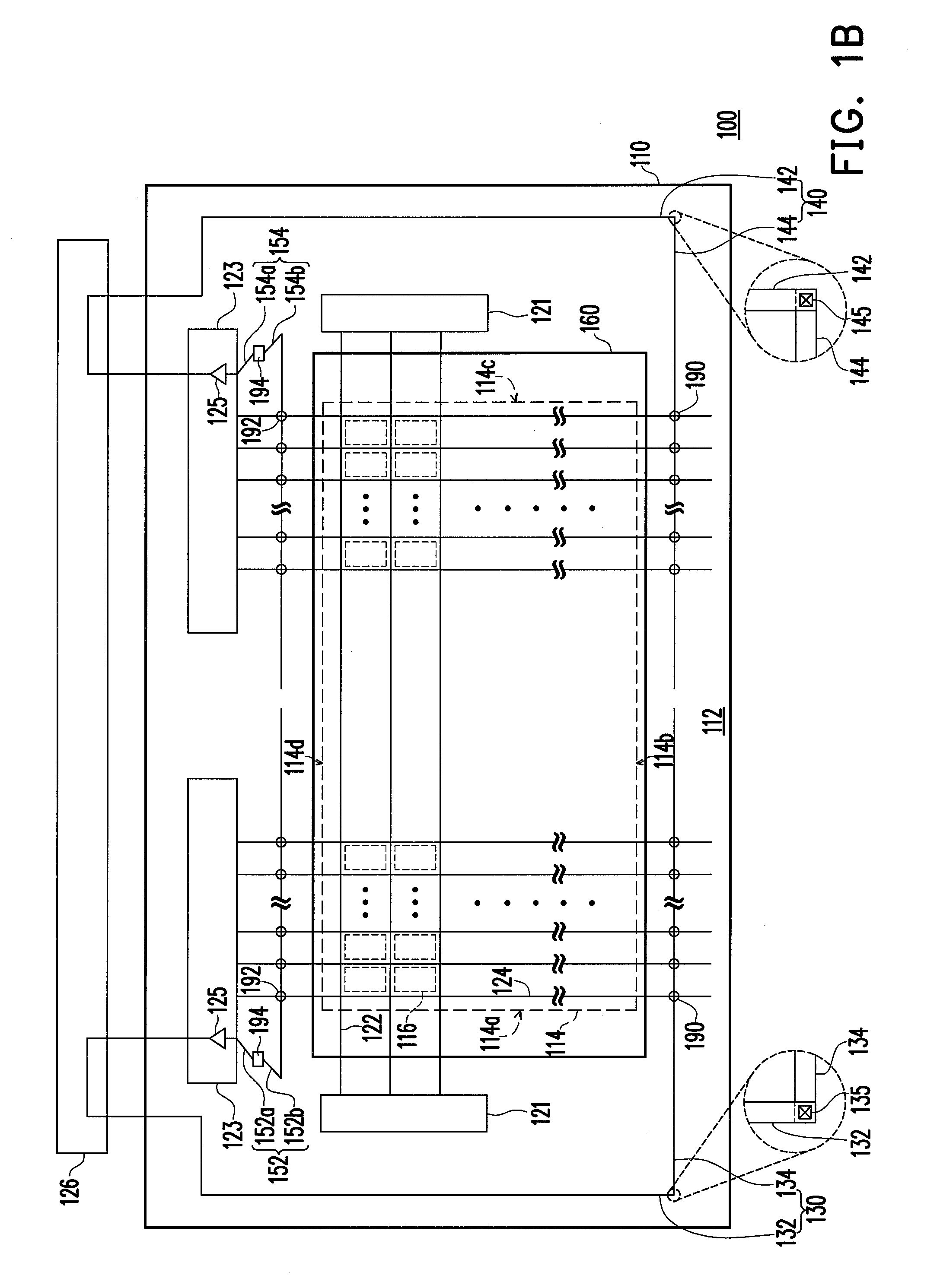
[0039]FIG. 1A is a schematic cross-sectional view illustrating a display panel according to a first embodiment of the invention. FIG. 1B is a schematic top view illustrating the display panel depicted in FIG. 1A. In FIG. 1B, the liquid crystal layer is not shown. With reference to FIG. 1A and FIG. 1B, a display panel 100 of this embodiment includes an active device array substrate 110, an opposite substrate 160, and a liquid crystal layer 170. The active device array substrate 110 includes a first substrate 112, a pixel array 114, a plurality of scan lines 122, a plurality of data lines 124, a first repairing line 130, and a second repairing line 140. The pixel array 114 is disposed on the first substrate 112. The pixel array 114 includes a plurality of pixels 116 arranged in array, and the pixels 116 include active devices (not shown) of thin film transistors and pixel electrodes (not shown) electrically connected to the active devices. The scan lines 122 and the data lines 124 are...

second embodiment

[0051]FIG. 3A is a schematic cross-sectional view illustrating a display panel according to a second embodiment of the invention. FIG. 3B is a schematic top view illustrating the display panel depicted in FIG. 3A. In FIG. 3B, the liquid crystal layer is not shown. With reference to FIG. 3A and FIG. 3B, in this embodiment, the display panel 100 includes an active device array substrate 110, an opposite substrate 160, and a liquid crystal layer 170. The active device array substrate 110 and the opposite substrate 160 have the same components as those described in the first embodiment, and therefore the detailed description thereof can refer to the abovementioned. The first repairing line 130 and the second repairing line 140 are described below.

[0052]The first repairing line 130 is disposed on the first substrate 112 and includes a first line segment 132 and a second line segment 134. The first line segment 132 is located at a first side 114a of the pixel array 114. The second line se...

third embodiment

[0060]FIG. 5A is a schematic cross-sectional view illustrating a display panel according to a third embodiment of the invention. FIG. 5B is a schematic top view illustrating the display panel depicted in FIG. 5A. In FIG. 5B, the liquid crystal layer is not shown. With reference to FIG. 5A and FIG. 5B, in this embodiment, the display panel 100 includes an active device array substrate 110, an opposite substrate 160, and a liquid crystal layer 170. The active device array substrate 110 and the opposite substrate 160 have the same components as those described in the first embodiment, and therefore the detailed description thereof can refer to the abovementioned. The first repairing line 130 and the second repairing line 140 are described below.

[0061]The first repairing line 130 is disposed on the first substrate 112 and includes a first line segment 132, a second line segment 134, a plurality of first sub-line segments 136, and a plurality of second sub-line segments 138. The first li...


PUM

PropertyMeasurementUnit
areaaaaaaaaaaa
lengthaaaaaaaaaa
capacitanceaaaaaaaaaa

Abstract

A display panel includes an active device array substrate, an opposite substrate, and a liquid crystal layer. The active device array substrate includes a substrate and further includes a pixel array, signal lines, and first and second repairing lines all disposed on the substrate. The signal lines electrically connect the pixel array. The first repairing line includes first and second line segments respectively located on first and second sides of the pixel array. The first side is substantially perpendicular to the second side. The first and second line segments are electrically connected. The second repairing line includes third and fourth line segments respectively located on third and second sides of the pixel array. The third side is substantially parallel to the first side. The fourth and third line segments are electrically connected. The opposite substrate above the active device array substrate does not cover the first and third line segments.

Description

CROSS-REFERENCE TO RELATED APPLICATION[0001]This application claims the priority benefit of Taiwan application serial no. 99128491, filed on Aug. 25, 2010. The entirety of the above-mentioned patent application is hereby incorporated by reference herein and made a part of this specification.BACKGROUND OF THE INVENTION[0002]1. Field of the Invention[0003]The invention relates to a panel. More particularly, the invention relates to a display panel.[0004]2. Description of Related Art[0005]In general, a liquid crystal display (LCD) panel is mainly comprised of an active device array substrate, an opposite substrate, and a liquid crystal layer sandwiched between the active device array substrate and the opposite substrate. The active device array substrate has a plurality of pixels arranged in an array, and each of the pixels includes an active device and a pixel electrode electrically connected to the active device. A plurality of scan lines and a plurality of data lines are disposed on...

Claims


Application Information

Patent Timeline
Patent Type & Authority Applications(United States)
IPC IPC(8): G02F1/1343
CPCG02F1/136259G02F2001/136272G02F2001/136263G02F2001/13606G02F1/13606G02F1/136263G02F1/136272
Inventor CHENG, MIEN-MIENLIAO, YI-SUEILIN, JIAN-HONGCHIU, CHIEN-FENG
Owner AU OPTRONICS CORP
Why Eureka
Try Eureka