Semiconductor device

Active Publication Date: 2012-03-01
SEMICON ENERGY LAB CO LTD
View PDF3 Cites 29 Cited by
  • Summary
  • Abstract
  • Description
  • Claims
  • Application Information

AI Technical Summary

Benefits of technology

[0022]A semiconductor device according to an embodiment of the present invention includes a memory cell which holds data in a node to which one of a source and a drain of a transistor whose channel region is formed from an oxide semiconductor is electrically connected. Note that the value of off-state current (leakage current) of the transistor is extremely small. Thus, after being set to have a predetermined value, the potential of the node can be kept constant or substantially constant by turning the transistor off. In this manner, accurate data can be stored in the memory cell.
[0023]The node is electrically connected to the one of the source and the drain of the transistor. Thus, the potential of the node can be easily controlled by transfer of electric charge

Problems solved by technology

An increase in storage capacity causes an increase in circuit size.
However, there is limitation on the amount of electric charge which can be held in the floating gate and the amo

Method used


Image

  • Semiconductor device
  • Semiconductor device
  • Semiconductor device

Examples


specific example 2

of Memory Cell 30

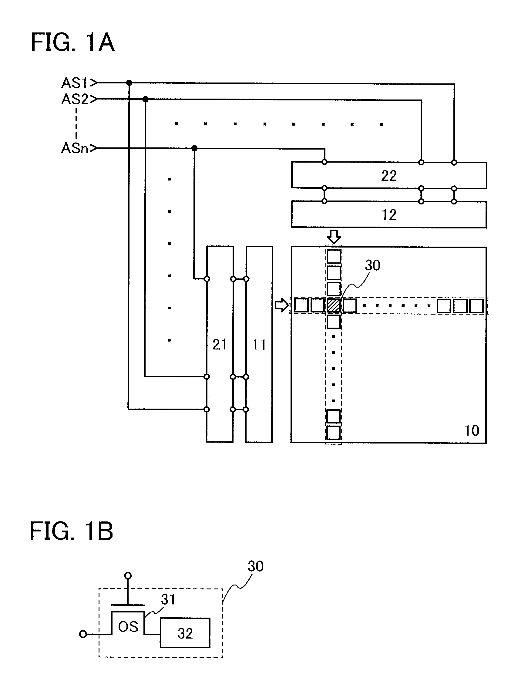
[0116]FIG. 9B is a circuit diagram illustrating a specific example of the memory cell 30, which is different from that in FIG. 9A. Each of the memory cells 30 in FIG. 9B is one of the memory cells 30 arranged in a line. The memory cell 30 includes the transistor 31, a transistor 40, and a capacitor 41. The gate of the transistor 31 is electrically connected to a writing word line 42, and one of the source and the drain of the transistor 31 is electrically connected to a bit line 44. A gate of the transistor 40 is electrically connected to the other of the source and the drain of the transistor 31. One electrode of the capacitor 41 is electrically connected to the other of the source and the drain of the transistor 31 and the gate of the transistor 40, and the other electrode of the capacitor 41 is electrically connected to a reading word line 43. In addition, one of the source and the drain of the transistor 40 included in the k-th (k is a natural number greater tha...


PUM


Abstract

An object is to provide a semiconductor device which includes a memory cell capable of holding accurate data even when the data is multilevel data. The semiconductor device includes a memory cell holding data in a node to which one of a source and a drain of a transistor whose channel region is formed from an oxide semiconductor. Note that the value of off-state current (leakage current) of the transistor is extremely small. Thus, after being set to have a predetermined value, the potential of the node can be kept constant or substantially constant by turning the transistor off. In this manner, accurate data can be stored in the memory cell.

Description

BACKGROUND OF THE INVENTION[0001]1. Field of the Invention[0002]The present invention relates to a semiconductor device using a semiconductor element. In particular, the present invention relates to a semiconductor device including a memory device using a semiconductor element. Note that the semiconductor device in this specification indicates all the devices that operate by utilizing semiconductor characteristics.[0003]2. Description of the Related Art[0004]Memory devices using semiconductor elements are broadly classified into two categories: a volatile device that loses stored data when power supply stops, and a non-volatile device that retains stored data even when power is not supplied.[0005]A typical example of a volatile memory device is a DRAM (dynamic random access memory). A DRAM stores data in such a manner that a transistor included in a memory cell is selected and electric charge is stored in a capacitor.[0006]When data is read from a DRAM, electric charge in a capacito...

Claims


Application Information

Patent Timeline
IPC IPC(8): G11C11/24G11C8/10H01L27/07
CPCG11C16/0433G11C16/08H01L27/11517H01L27/1225G11C13/003G11C11/565G11C11/5685G11C13/0004G11C11/403H10B41/00H10B99/00H10B12/00
Inventor YAMAZAKI, SHUNPEIKOYAMA, JUN
Owner SEMICON ENERGY LAB CO LTD
Why Eureka
Try Eureka