Sensing structure of alignment of a probe for testing integrated circuits

a technology for integrated circuits and sensing structures, which is applied in the direction of mechanical vibration separation, biochemistry apparatuses and processes, instruments, etc., can solve the problems of not being able to determine the drift direction of the probe, the possibility of damaging the passivation surrounding the pad, and the height of the probe, so as to reduce the dimension

Active Publication Date: 2012-03-22
STMICROELECTRONICS SRL
View PDF10 Cites 49 Cited by
  • Summary
  • Abstract
  • Description
  • Claims
  • Application Information

AI Technical Summary

Benefits of technology

[0017]Given these problems with the existing technology, it would be advantageous to provide a sensing structure that has reduced dimensions and is capa...

Problems solved by technology

Consequently the probability of damaging the passivation surrounding the pad, due to a not properly performed probing, becomes higher.
However, the dummy pad 10 illustrated in FIG. 34 only allows detecting whether the probe contacts the sensing structures within or outside the probing area but does not allow determining the drift direction of the probe.
However, in the testing process, it often occurs that the probe tip does not contact the corresponding connection terminal perfectly, due, for instance, to oxidation of the tip itself or to imperfections of the pad.
Consequently, the structures described in the cited prior art documents are either not capable of determining the drift direction of the probe or will fail to correctly determine the position of the probe in a significant number of measurements.
M...

Method used


Image

  • Sensing structure of alignment of a probe for testing integrated circuits
  • Sensing structure of alignment of a probe for testing integrated circuits
  • Sensing structure of alignment of a probe for testing integrated circuits

Examples


Embodiment Construction

[0055]In the following description, for explanatory purposes, specific details are set forth in order to provide a thorough understanding of the ideas of the present invention. However, it may be evident that the present invention can be practiced without using these specific details. Furthermore, well know structures and devices are only described in general form in order to facilitate the description thereof.

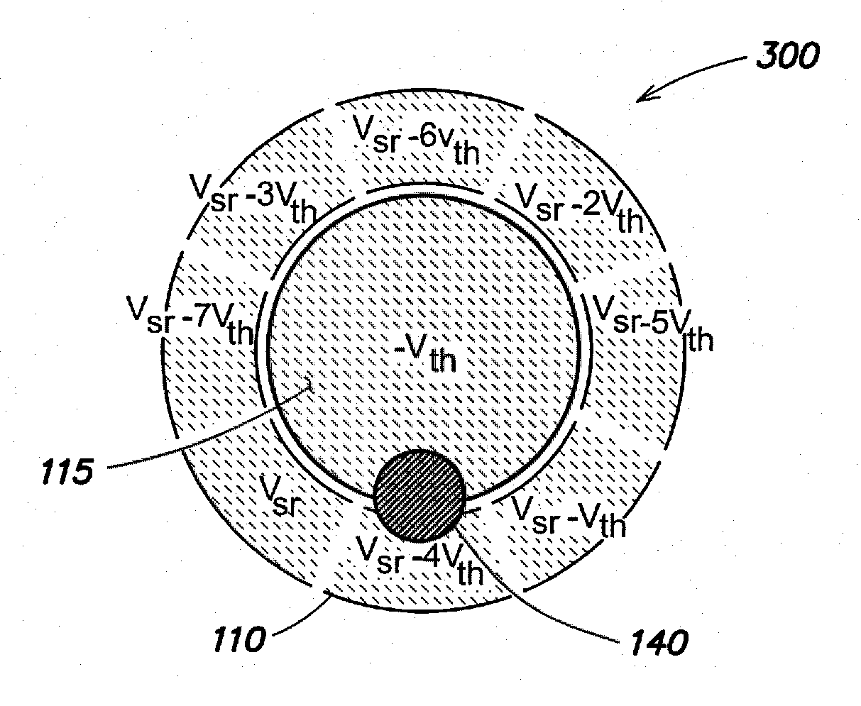
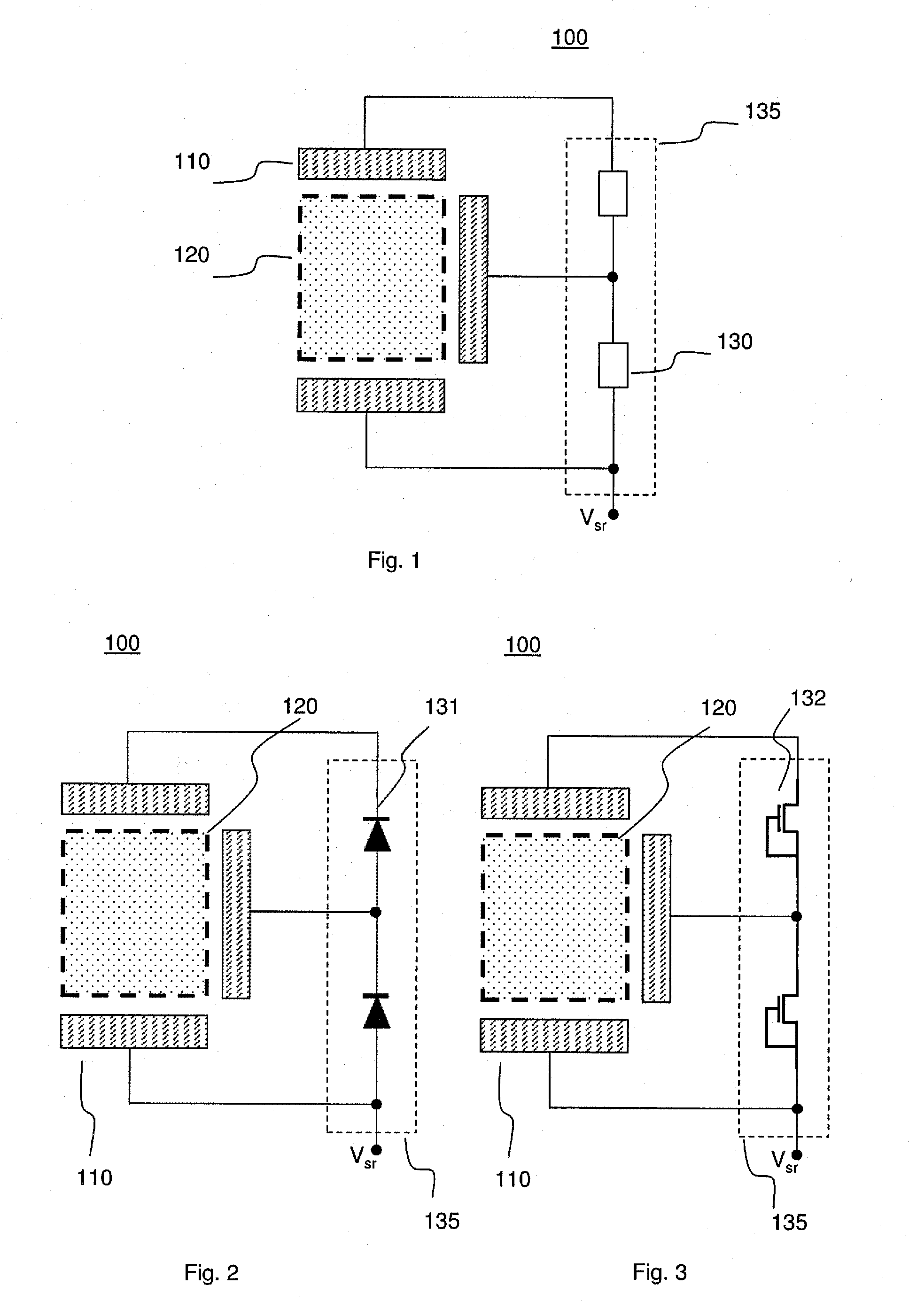
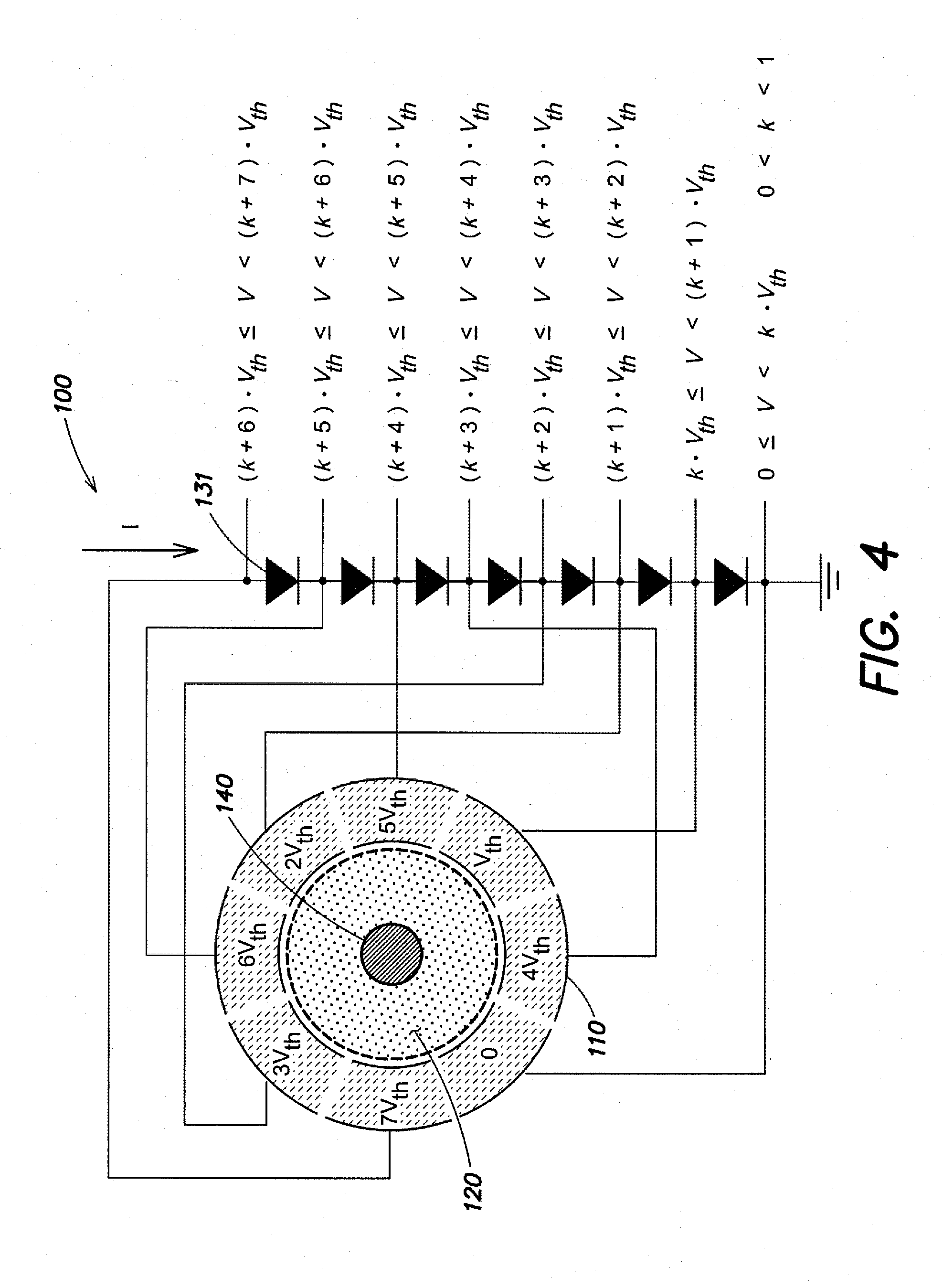
[0056]One problem is based on the observation that with the progress in photo-lithographic technologies, substrates for integrated circuits, such as wafers including integrated circuits, include an increasingly large number of connecting pads closely arranged next to each other. Correctly aligning a probe with the corresponding connection terminal on the substrate during the testing phase has therefore become crucial in order not to damage the area surrounding the connection terminal itself. Said connection terminal may be, for instance, a pad or a bump (protruding contact bum...


PUM


Abstract

A sensing structure for use in testing integrated circuits on a substrate. The sensing structure includes at least two sensing regions connectable to a probe and at least one first sensing element. Each of the at least one first sensing elements is directly connected to two sensing regions such that for each sensing region a different value of an electrical parameter is measurable between the sensing region and a first reference potential so as to reliably determine a drift direction of a probe.

Description

CROSS REFERENCE TO RELATED APPLICATIONS[0001]This application claims the priority benefit of Italian patent application number VI2010A000159, filed on Jun. 10, 2010 entitled SENSING STRUCTURE OF ALIGNMENT OF A PROBE FOR TESTING INTEGRATED CIRCUITS, which is hereby incorporated by reference to the maximum extent allowable by law.BACKGROUND OF THE INVENTION[0002]1. Field of the Invention[0003]The present invention relates to a structure for use in testing electronic components in a substrate. Moreover, the present invention relates to a substrate including one or more sensing structures and a testing equipment for testing electronic components on a substrate.[0004]2. Discussion of the Related Art[0005]Thanks to the advance in the field of manufacturing processes of electronic integrated circuits, electrical components have become smaller, thereby allowing manufacturing substrates including a large number of integrated circuits. Moreover, it is possible to fabricate compact electronic ...

Claims


Application Information

Patent Timeline
IPC IPC(8): G01R31/26
CPCG01R1/06794H01L22/34G01R31/2891G01R31/2884B06B2201/00C12Q1/00C12Q2304/00C12Q2326/00G01N1/00G01R11/00H01L21/00H01L2221/00H01L2924/00
Inventor PAGANI, ALBERTO
Owner STMICROELECTRONICS SRL
Why Eureka
Try Eureka