Semiconductor storage device and data control method thereof

a technology of semiconductor storage device and data control method, which is applied in the direction of memory address/allocation/relocation, instruments, computing, etc., can solve the problems of reducing device performance and long time taken to erase flash memory, and achieve the effect of prolonging the operating life of the devi

Inactive Publication Date: 2012-03-22
HITACHI LTD
View PDF9 Cites 54 Cited by
  • Summary
  • Abstract
  • Description
  • Claims
  • Application Information

AI Technical Summary

Benefits of technology

[0019]According to the present invention, the number of times the physical blocks belonging to the flash memory are erase targets can be reduced in order to prolong a longer device operating life.

Problems solved by technology

However, the time taken to erase flash memory is long compared to the write time, which greatly lowers the device performance, and therefore a method is typically adopted for a data update, whereby, once the recorded data has been read, update data is generated integrally with the write data, the generated update data is written to another unwritten area, and the original recorded area is invalidated (a process which renders the host system unable to reference this area).
However, with flash memory, since the minimum erase unit is large in comparison with the minimum write unit, an erased area may sometimes include an area (valid area) which stores valid data which has not been invalidated.

Method used


Image

  • Semiconductor storage device and data control method thereof
  • Semiconductor storage device and data control method thereof
  • Semiconductor storage device and data control method thereof

Examples


example 1

[0042]The first embodiment (Example 1) is configured such that the physical blocks, which are batch erase units among the data storage areas of the flash memory, are each divided into a base area which is a storage destination of new write data and an update area which is a storage destination of update data, and a physical page, which is a minimum write unit, is divided into a plurality of pages in the base area and the update area respectively, and when data is stored on any of the physical pages of a physical block based on a write request, the write data added to the write request is compressed, and on condition that the physical pages serving as write targets are reduced, the compressed data is stored on any of the physical pages, the number of physical pages assigned to the base area belonging to the physical block is reduced, and the number of physical pages assigned to the update area of the physical block is increased.

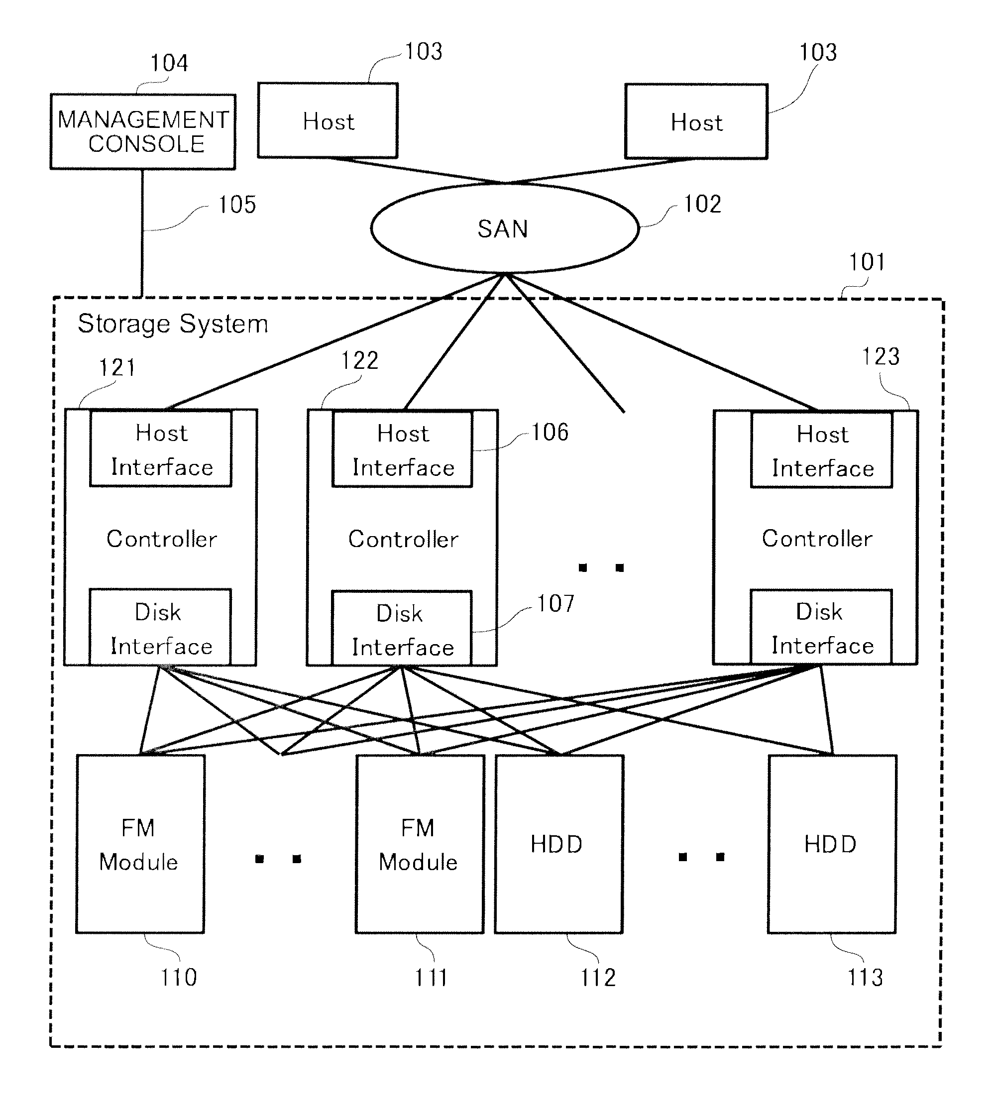
[0043]FIG. 1 is a schematic configuration diagram of a c...

example 2

[0214]A flash module according to a second embodiment ample 2) will be explained next. The second embodiment is the same as the first embodiment with regard to the address conversion management information (LBA / PBA conversion management information) 600, the update area management information 800, and the read / write operation of the flash module 110 and therefore an explanation of these elements is not included here.

[0215]In the second embodiment, data compression is performed in the event of data compression during a data write according to the first embodiment, but also for a reclamation operation and refresh operation. In addition, the read frequencies of the PBA group to be compressed during data compression is referred to and only those PBA groups with a low read frequency are compressed.

[0216]According to the second embodiment, the data with a high read frequency is stored in the flash memory in an uncompressed form, and a performance drop which is inevitably produced by the o...

example 3

[0277]In the first and second embodiments, the LBA and PBA are managed separately with areas of a fixed size serving as the LBA groups and areas of the physical block size serving as PBA groups, and optional PBA groups are assigned to the LBA groups However, in the third embodiment (Example 3), an example is shown in which the physical page size units which are the minimum read / write units of the flash memory are managed separately as LBA Pages and PRA Pages, optional PBA Pages are assigned to the LBA Pages, and data compression is applied to this address conversion management configuration.

[0278]The third embodiment is the same as the first embodiment and second embodiment with regard to device configuration and erase management information, therefore a description is omitted.

[0279]FIG. 16 is a conceptual view which conceptually shows correspondence between an LBA space and PBA space according to the third embodiment.

[0280]As shown in FIG. 16, in the third embodiment, the LBA space...


PUM


Abstract

The flash memory controller compresses data in response to a write request. On condition that there is a compression effect with respect to the compressed data, the flash memory controller writes the compressed data to the base area of a physical block of a flash memory. As physical pages assigned to the physical block, the flash memory controller reduces the physical pages assigned to the base area from 102 down to 59, and increases the physical pages assigned to the update area from 26 up to 69. Therefore, it is possible to suppress exhaustion of physical pages which are assigned to the update area, to reduce the number of erases of the physical block, and to consequently prolong device operating life.

Description

TECHNICAL FIELD[0001]The present invention relates to a semiconductor storage device and, more particularly, to a semiconductor storage device and data control method thereof comprising a data input and output processing function for a storage device which includes, as a storage medium, a flash memory which is one type of involatile memory that is electrically rewritable.BACKGROUND ART[0002]Flash memory is characterized by the fact that data cannot be rewritten to a data area that has already been recorded. For this reason, in order to update recorded data, processing is required to erase a recorded area after reading the recorded data and then write update data to the erased unwritten area.[0003]However, the time taken to erase flash memory is long compared to the write time, which greatly lowers the device performance, and therefore a method is typically adopted for a data update, whereby, once the recorded data has been read, update data is generated integrally with the write dat...

Claims


Application Information

Patent Timeline
Patent Type & Authority Applications(United States)
IPC IPC(8): G06F12/02
CPCG06F3/0608G06F3/0688G06F3/064G06F12/0246G06F2212/1036G06F2212/401G06F2212/7201G06F2212/7203G06F2212/7205G06F2212/7208
Inventor SUZUKI, AKIFUMIKAWAMURA, ATSUSHIOGAWA, JUNJI
Owner HITACHI LTD
Why Eureka
Try Eureka