Trench mosfet with super pinch-off regions

Inactive Publication Date: 2012-04-05
FORCE MOS TECH CO LTD
View PDF6 Cites 39 Cited by
  • Summary
  • Abstract
  • Description
  • Claims
  • Application Information

AI Technical Summary

Benefits of technology

[0005]It is therefore an object of the present invention to provide a new and improved semiconductor power device such as a trench MOSFET with trenched source-body contact structure and super pinch-off regions for better pinch-off performance. In an N-channel trench MOSFET, super pinch-off regions are implemented by forming two type pinch-off regions as shown in FIG. 2: wherein a first type pinch-off region R1 with a wide mesa width Wm1<1.3 um is generated between the lower portion of two adjacent trenched gates and below an anti-PT (anti-Punch Through)

Problems solved by technology

The N-channel trench MOSFET of prior art in FIG. 1 has one electric field pinch-off region between two adjacent of the trenched gates, allowing short channel length formation without having severe punch-through problem, however, there are still some disadvantage constraining performance of the trench MOSFET.
The prior art used a planar contact structure for source-body contact in a mesa between every two adjacent of the

Method used


Image

  • Trench mosfet with super pinch-off regions
  • Trench mosfet with super pinch-off regions
  • Trench mosfet with super pinch-off regions

Examples


Embodiment Construction

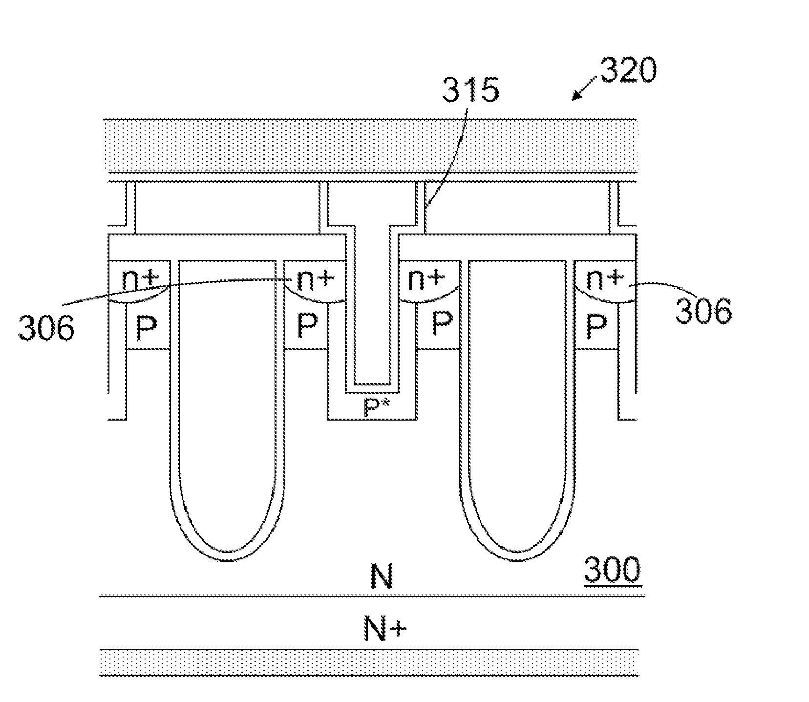
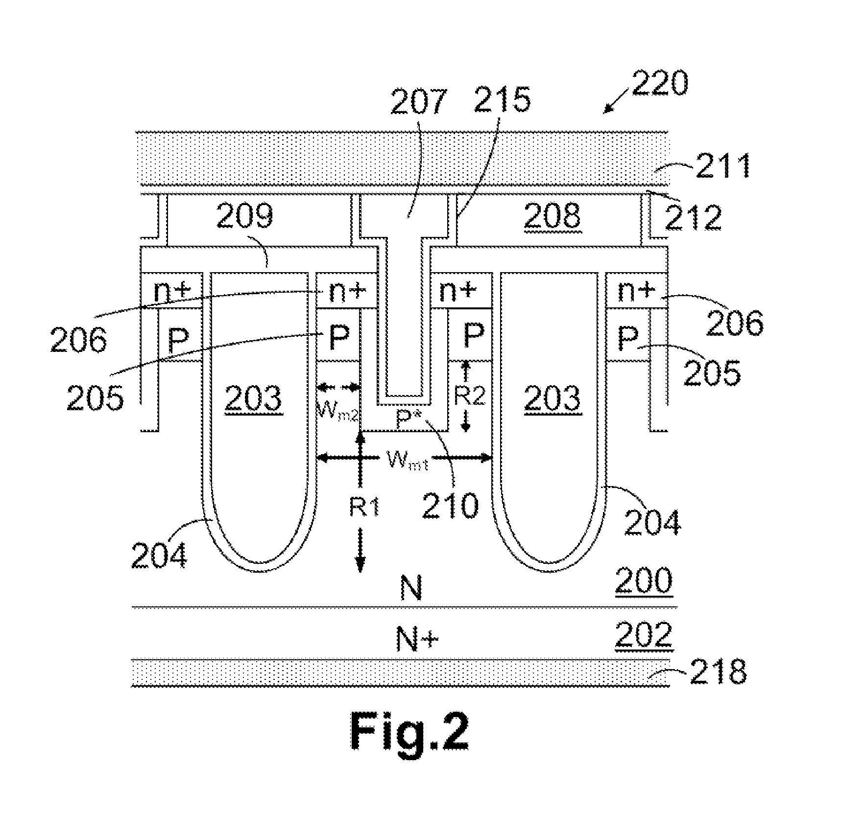
[0027]Please refer to FIG. 2 for a preferred N-channel trench MOSFET 220 with super pinch-off regions according to the present invention. The N-channel trench MOSFET 220 is formed in an N epitaxial layer 200 supported on a heavily doped N+ substrate 202 which coated with back metal 218 on the rear side as drain. A plurality of trenched gates are extending from the top surface of the N epitaxial 200, wherein each of the trenched gates filled with n+ or p+ doped poly-silicon 203 padded by a single gate oxide layer 204. In a wide mesa defined by an area between two adjacent of the trenched gates, a P body region 205 is formed below n+ source region 206 which near the top surface of the mesa. A trenched source-body contact 215 having vertical sidewall and filled with tungsten plug 207 padded by a barrier layer of Ti / TiN or Ta / TiN or Co / TiN is penetrating through a contact interlayer comprising a BPSG layer 208 and a NSG layer 209 beneath, further through the n+ region 206, the P body re...


PUM


Abstract

A trench MOSFET with short channel length and super pinch-off regions is disclosed, wherein the super pinch-off regions are implemented by forming at least two type pinch-off regions for punch-through prevention: a first type pinch-off region with a wide mesa width generated between lower portion of two adjacent trenched gates and below an anti-punch through region surrounding bottom of a trenched source-body contact filled with metal plug; a second type pinch-off region with a narrow mesa width generated below a body region and between upper portion of one trenched gate and the anti-punch-through region along sidewall of the trenched source-body contact.

Description

FIELD OF THE INVENTION[0001]This invention relates generally to the cell structure, device configuration and fabricating method of semiconductor devices. More particularly, this invention relates to an improved trench MOSFET (Metal Oxide Semiconductor Field Effect Transistor) configuration with short channel length having super pinch-off regions for Idsx (leakage current between drain and source) reduction.BACKGROUND OF THE INVENTION[0002]Please refer to FIG. 1 for an N-channel trench MOSFET of prior art (U.S. Pat. No. 6,285,060) formed in an N− drift region 100 onto an N+ substrate 102. A plurality of trenched gates are filled with doped poly-silicon 103 padded by a gate oxide layer 104, wherein the portion of the gate oxide layer on bottom of the trenched gates is thicker than that along sidewall of the trenched gates for Qgd (charge between gate and drain) reduction. P body region 105 is shallow, defining a short channel length between N+ source region 106 and the N− drift region...

Claims


Application Information

Patent Timeline
IPC IPC(8): H01L29/78H01L21/336
CPCH01L21/26586H01L29/0623H01L29/086H01L29/0869H01L29/1095H01L29/407H01L29/7813H01L29/4236H01L29/42368H01L29/456H01L29/66727H01L29/66734H01L29/7811H01L29/41766
Inventor HSIEH, FU-YUAN
Owner FORCE MOS TECH CO LTD
Why Eureka
Try Eureka