Method for cutting liquid crystal panel and method for manufacturing liquid crystal panel using the same

a technology manufacturing method, which is applied in the manufacture of electrode systems, instruments, electric discharge tubes/lamps, etc., can solve the problems of display signal lines or thin film transistors on the lower display panel being damaged, and errors in the manufacturing of liquid crystal display panel

Active Publication Date: 2012-04-05
TOVIS
View PDF1 Cites 8 Cited by
  • Summary
  • Abstract
  • Description
  • Claims
  • Application Information

AI Technical Summary

Benefits of technology

[0013]According to a present invention, in the cutting of a liquid crystal display panel which includes an upper panel to which a color filter is formed and a lower filter on which a thin film transistor is formed, the cut edge of the upper panel is upwardly protruded from the cut edge of the lower panel, so electrodes, signal lines, thin film transistors of the lower panel can be prevented from being damaged by the contact with the dispenser or by the pressure of the sprayed sealant while the sealant is formed after the cutting.

Problems solved by technology

Generally, a liquid crystal display panel has one of some standardized sizes, so use of the liquid crystal panel for various purposes is limited by the standardized size.
At this time, the sealant layer is formed by moving a dispenser for spraying sealant along the cut portion, and during this process, the display signal lines or the thin film transistors on the lower display panel may be damaged by contact of the dispenser and the lower display panel or pressure of the sprayed sealant.
The damage of the display signal lines or the thin film transistors may cause an error in the manufactured liquid crystal display panel.

Method used


Image

  • Method for cutting liquid crystal panel and method for manufacturing liquid crystal panel using the same
  • Method for cutting liquid crystal panel and method for manufacturing liquid crystal panel using the same
  • Method for cutting liquid crystal panel and method for manufacturing liquid crystal panel using the same

Examples


Embodiment Construction

Technical Problem

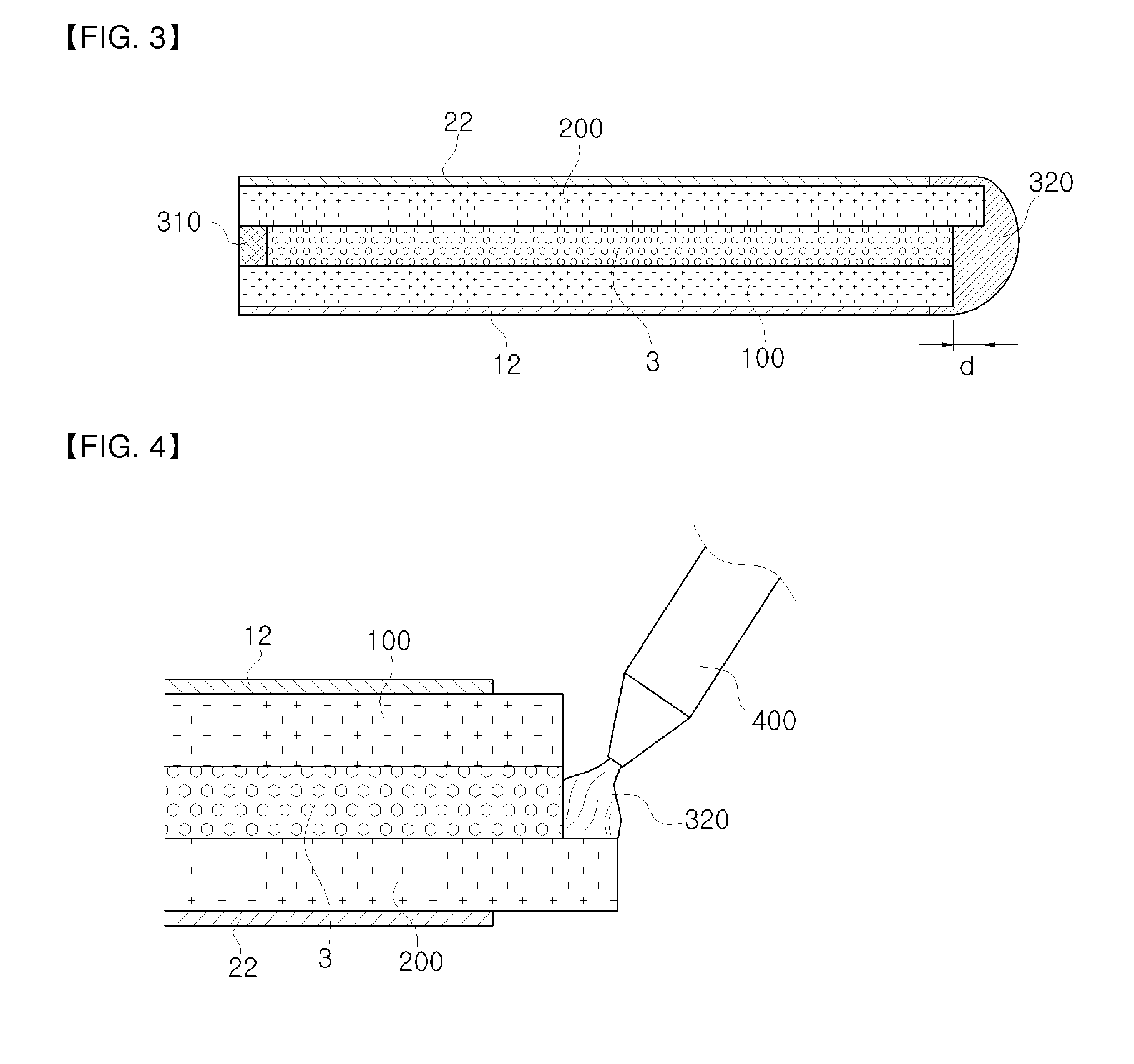
[0007]The present invention has been made in an effort to provide a method for cutting a liquid crystal display panel in which damages on signal lines or thin film transistors which are formed on a lower panel during the process of forming a sealant which is needed for cutting a liquid crystal display panel can be minimized.

Technical Solution

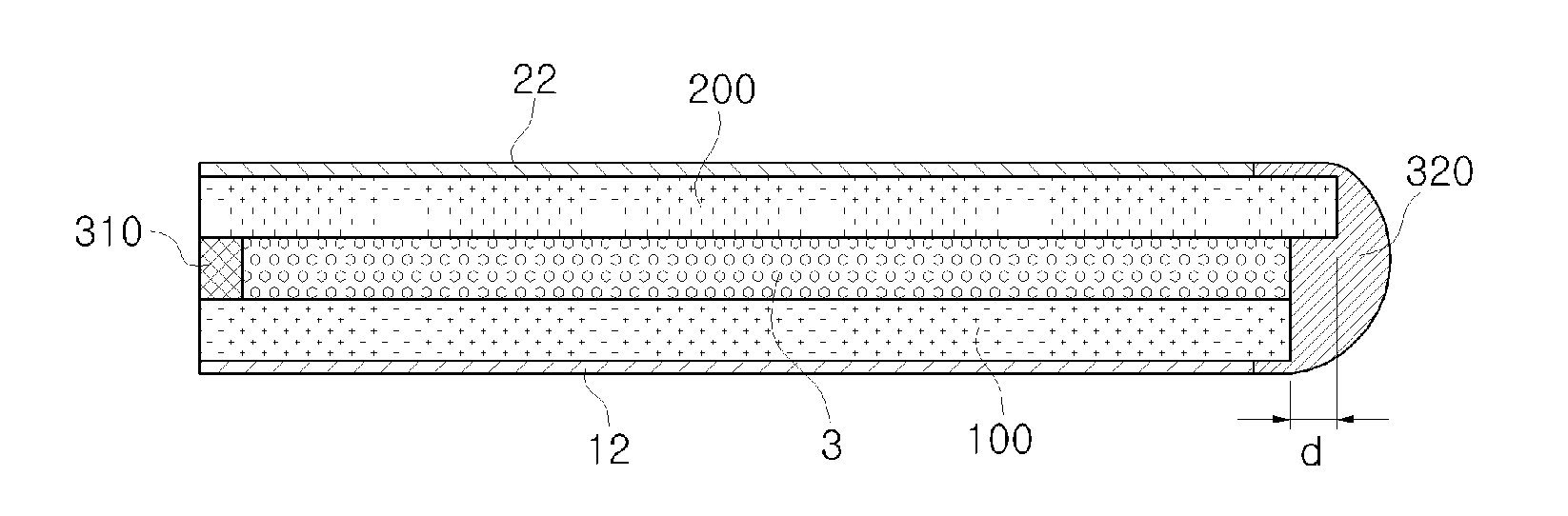
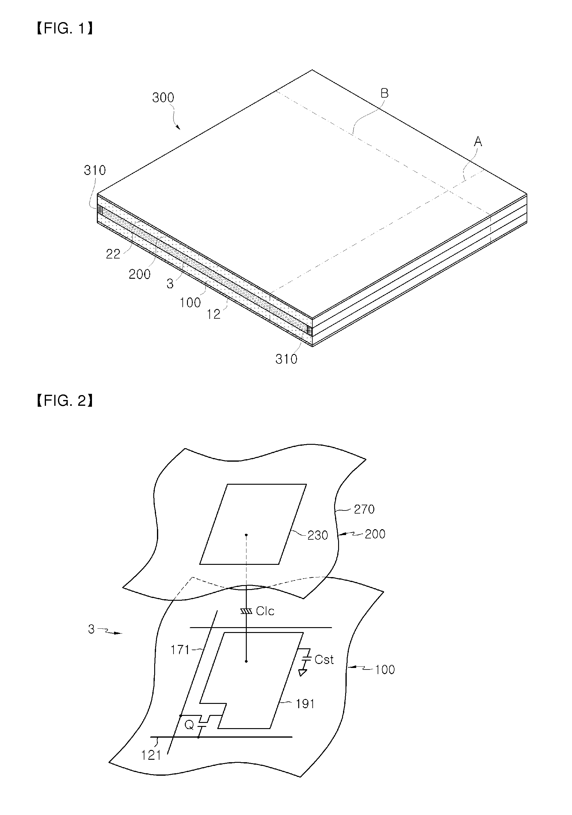
[0008]According to an embodiment of the present invention, in a method for cutting a liquid crystal display panel which includes an upper panel to which a color filter is formed and a lower filter on which a thin film transistor is formed, the upper panel and the lower panel are respectively cut in such a way that a cut edge of the upper panel is outwardly protruded from a cut edge of the lower panel so that a step is formed at a cut surface between the upper panel and the lower panel.

[0009]The upper panel and the lower panel may be respectively cut such that the cut edge of the upper panel is outwardly protruded from the cut ed...


PUM


Abstract

The present invention relates to a method for cutting a liquid crystal display panel and a method for manufacturing a liquid crystal display panel having a desired size using the same. In a method for cutting a liquid crystal display panel which includes an upper panel to which a color filter is formed and a lower filter on which a thin film transistor is formed, the upper panel and the lower panel are respectively cut in such a way that a cut edge of the upper panel is outwardly protruded from a cut edge of the lower panel so that a step is formed at a cut surface between the upper panel and the lower panel. Since the cut edge of the upper panel is upwardly protruded from the cut edge of the lower panel, electrodes, signal lines, thin film transistors of the lower panel can be prevented from being damaged by the contact with the dispenser or by the pressure of the sprayed sealant while the sealant is formed after the cutting.

Description

FIELD OF THE INVENTION[0001]The present invention relates to a method for cutting a liquid crystal display panel and a method for manufacturing a liquid crystal display panel having a desired size using the same.Background Art[0002]Generally, a liquid crystal display (LCD) includes two display panels and a liquid crystal layer disposed therebetween and having a dielectric anisotropy. An electric filed is formed in the liquid crystal layer, and a transmittance of light passing the liquid crystal layer is regulated by regulating amplitude of the electric field so as to obtain a desired image. Such a liquid crystal display is representative one of a flat panel display (FPD), and TFT-LCD which uses thin film transistor (TFT) as a switching element is widely used.[0003]A plurality of display signal lines i.e., gate lines and data lines, a plurality of thin film transistors and pixel electrodes are formed on a lower display panel of the two display panels of the liquid crystal display pan...

Claims


Application Information

Patent Timeline
Patent Type & Authority Applications(United States)
IPC IPC(8): H01J9/26H01J9/00
CPCG02F1/133351C03B33/076C03B33/02G02F1/13
Inventor KIM, YONG BEOMKIM, DONG HYUN
Owner TOVIS
Why Eureka
Try Eureka