Magnetic-electric energy conversion device, power supply device, and magnetic sensor
- Summary
- Abstract
- Description
- Claims
- Application Information
AI Technical Summary
Benefits of technology
Problems solved by technology
Method used
Image

Examples
embodiment
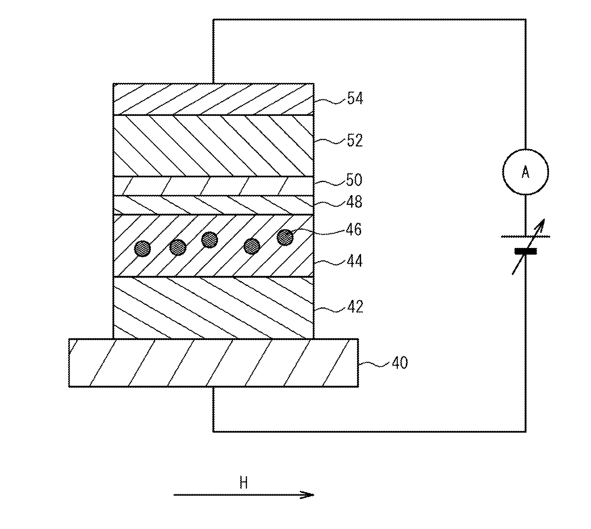
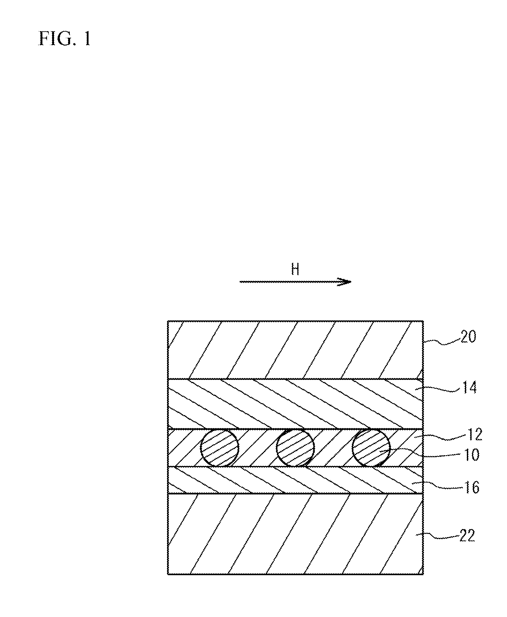
[0036]FIG. 5 is a schematic cross-sectional view of a magnetic-electric energy conversion device according to an example. As shown in FIG. 5, a Be-doped p-type GaAs layer 42 is formed on the (001) plane of a p-type GaAs substrate 40 by MBE (Molecular Beam Epitaxy) at a substrate temperature of 580° C. The film thickness of the p-type GaAs layer 42 is 20 nm.
[0037]After the p-type GaAs layer 42 is grown, the substrate temperature is lowered to 240° C., and a 10-nm thick Ga0.94Mn0.06As layer is formed on the p-type GaAs layer 42. An AlAs barrier layer 48 is formed on the Ga0.94Mn0.06As layer by MBE. The film thickness of the AlAs barrier layer 48 is 2.1 nm. A GaAs spacer layer 50 is formed on the AlAs barrier layer 48 by MBE. The film thickness of the GaAs spacer layer 50 is 1 nm. After that, the substrate temperature is increased to 480° C. in the MBE chamber, and a 20-minute heat treatment is performed. Through the treatment, a GaAs matrix layer 44 containing MnAs ferromagnetic parti...
PUM
 Abstract
Description
Claims
Application Information