Input device and method of producing input apparatus

a technology of input device and input device, which is applied in the direction of instruments, fluid pressure measurement, synthetic resin layered products, etc., can solve the problems of reducing reliability, affecting the operation of the input device, so as to achieve the effect of easy production of good visibility to the operator, extremely precise thickness of decorative layer, and easy control of thickness of transparent filler

Active Publication Date: 2012-04-26
ALPS ALPINE CO LTD
View PDF2 Cites 35 Cited by
  • Summary
  • Abstract
  • Description
  • Claims
  • Application Information

AI Technical Summary

Benefits of technology

[0030]With the method of producing an input device according to the present invention, it is preferable that, in step a, an inclination angle of the inclined section and the second surface of the transparent member be in a range of 30° to 60°. In this way, the thickness of the decorative layer can be controlled extremely precisely. In Step c of leveling the transparent filler, bubble formation in the light-transmissive region near the unlevel sections of the decorative layer can be reliably prevented, and the thickness of the transparent filler can be controlled extremely precisely.
[0031]It is preferable that, in step b, the transparent filler be a transparent resin. In this way, an input device providing good visibility to the operator can be easily produced.
[0032]It is preferable that, in step b, the transparent filler be applied by a printing method. In this way, the transparent filler can be easily applied by a printing method, such as screen printing or ink-jet printing.
[0033]It is preferable that, in step d, the transparent filler be cured by irradiating the transparent filler with ultraviolet rays. In this way, since curing at normal temperature is possible, without applying heat, an input device can be produced in a shorter amount of time at lower cost.
[0034]It is preferable that, in Step e, the sensor member be a capacitance tough sensor. In this way, a thin capacitance touch panel without bubbles in the light-transmissive region when viewed from the outside can be produced.
[0035]It is preferable that, in Step e, the sensor member be a resistive tough sensor. In this way, a thin resistive touch panel without bubbles in the light-transmissive region when viewed from the outside can be produced.

Problems solved by technology

Having an unlevel section is undesirable for good external appearance because the decorative printing sheet 141a disposed on the input-surface side of the input device 101 is directly viewed from the outside.
If the upper transmissive substrate 131 warps due to the influence of the unlevel section 123, problems, such as separation of the upper transmissive substrate 131 and reduction in reliability, occur.
Therefore, reducing the thickness of the adhesive layer 151 causes a great problem in reducing the thickness of the input device 101.
The problems described above are an issue in not only the resistive touch panel but also in, for example, capacitance type, electromagnetic induction type, optical type, and other types of input devices.

Method used


Image

  • Input device and method of producing input apparatus
  • Input device and method of producing input apparatus
  • Input device and method of producing input apparatus

Examples


first embodiment

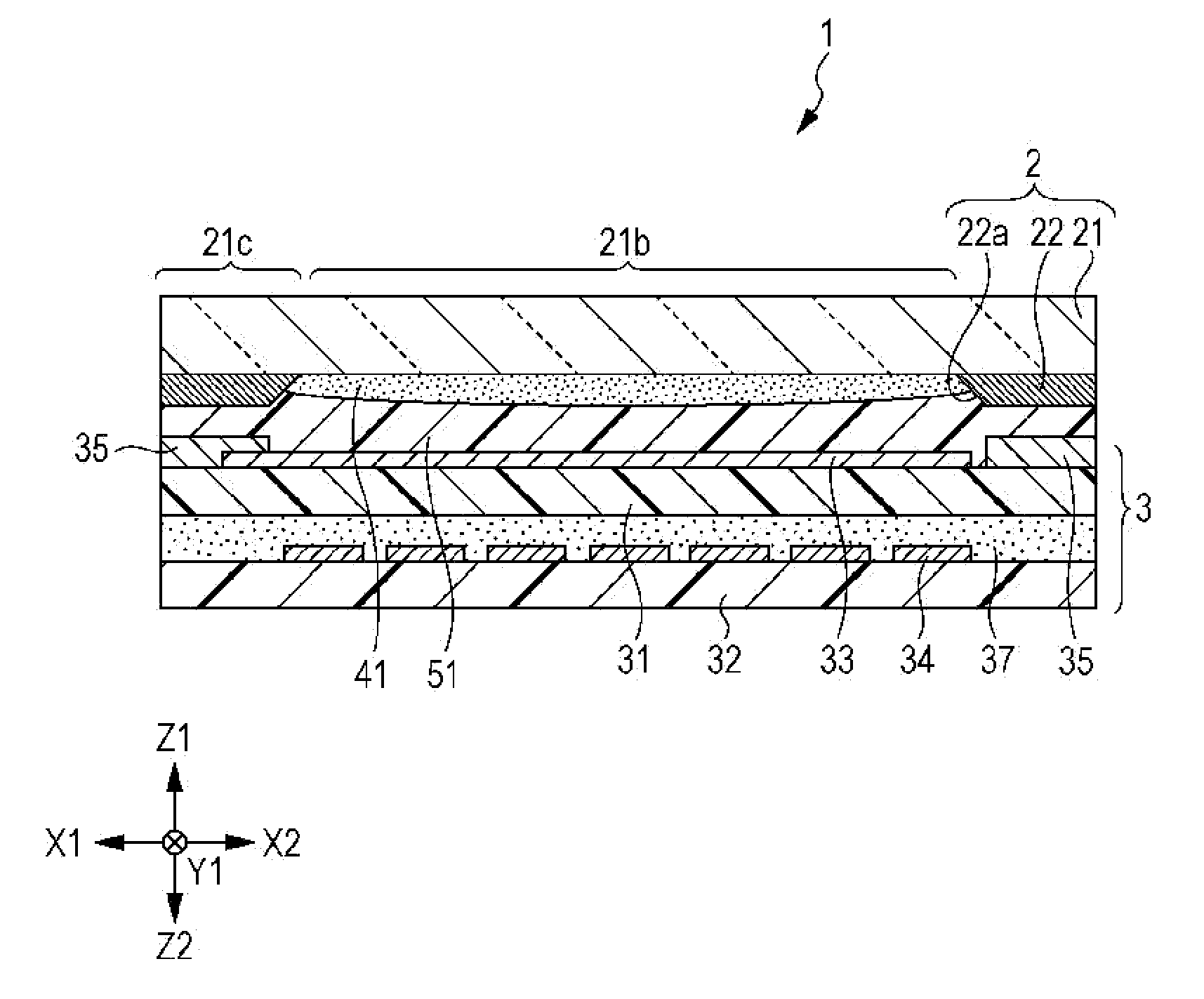
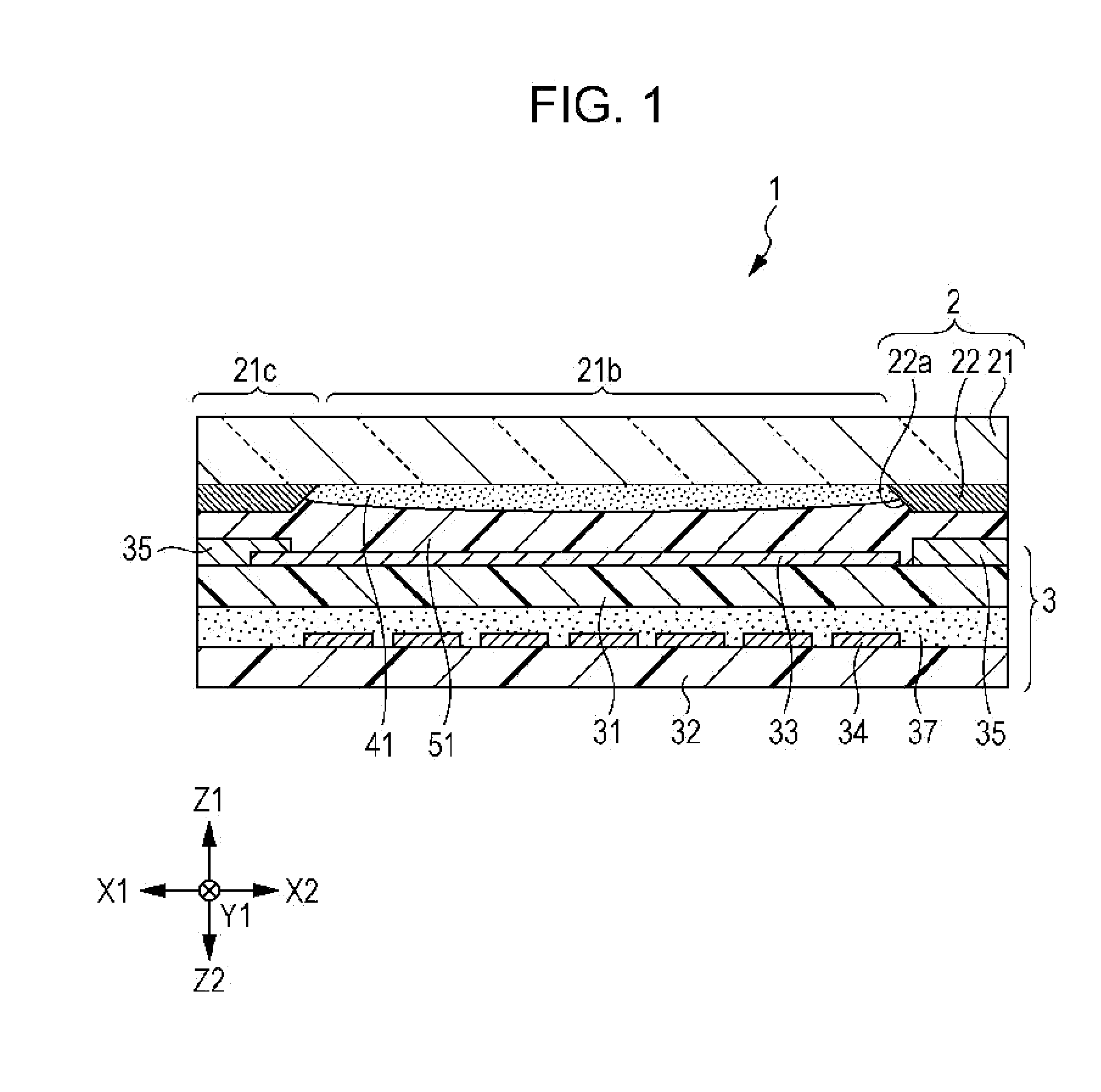
[0049]FIG. 1 is a sectional view of an input device 1 according to a first embodiment of the present invention. The input device 1 is mounted on a display unit in any electronic apparatus among a variety of electronic apparatuses, such as mobile phones and portable information terminals, such that the input device 1 covers the display screen of a display device, such as a liquid crystal panel. An operator can visibly confirm images on the display device through the input device 1 and can perform input operation by directly touching the display screen.

[0050]As illustrated in FIG. 1, the input device 1 includes a sensor member 3 configured to detect input position information and a protective member configured to protect the surface of the sensor member 3. The sensor member 3 and the protective member 2 are bonded together with a transparent filler 41 and an adhesive layer 51 interposed therebetween.

[0051]The sensor member 3 is a capacitance touch sensor configured to detect input pos...

second embodiment

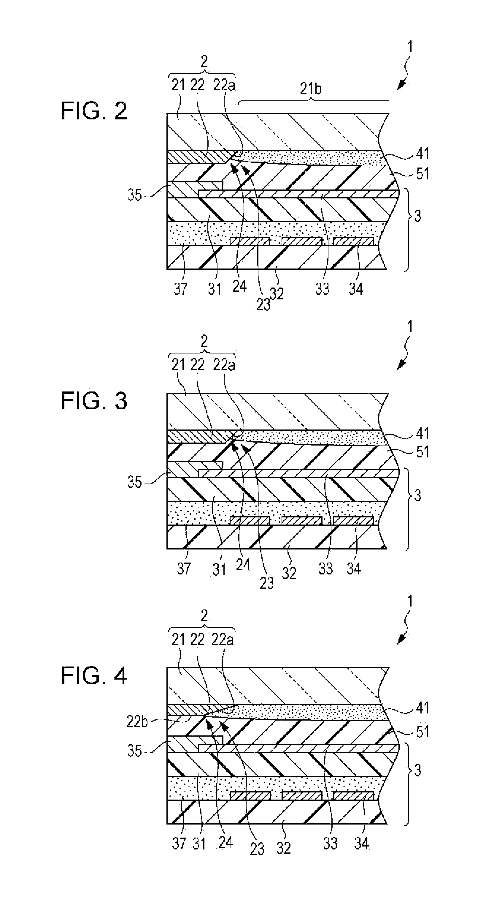
[0079]FIG. 7 is a sectional view of an input device 1 according to a second embodiment. In the input device 1 of the second embodiment, similar to that of the first embodiment, a protective member 2 and a sensor member 3 are bonded together with a transparent filler 41 and an adhesive layer 51 disposed therebetween, and the sensor member 3 constitutes a capacitance touch sensor.

[0080]In the second embodiment, a first wiring pattern 35 is disposed on the periphery of the first sensor substrate 31, and a protective layer 42 covers the top of the first wiring pattern 35. In the input device 1, to increase a light-transmissive region 21b, the first wiring pattern 35 has fine wiring such that a non-transmissive region 21c is decreased. Therefore, the protective layer 42 is provided on the first wiring pattern 35 to prevent wire breaking and short-circuiting. The protective layer 42 is made of the same resin as the transparent filler 41 using a printing method, such as screen printing or ...

third embodiment

[0083]FIG. 8 is a sectional view of an input device 1 according to a third embodiment. As illustrated in FIG. 8, a sensor member 3 in the third embodiment constitutes a resistive touch sensor. In the sensor member 3 in this embodiment, a first sensor substrate 31 and a second sensor substrate 32 oppose each other with a spacer 38 interposed therebetween. A first electrode pattern 33 and a second electrode pattern 34 are respectively disposed on the opposing surfaces of the first sensor substrate 31 and the second sensor substrate 32.

[0084]The first sensor substrate 31 disposed on the input-surface side is made of a flexible film of a transparent resin, such as polyethylene terephthalate (PET), and is deformable in response to input operation. The thickness of the first sensor substrate 31 is in the range of approximately 100 to 200 μm, e.g., 188 μm. The second sensor substrate 32 is made of transparent resin, such as polycarbonate (PC), polyethylene terephthalate (PET), polyether su...


PUM

PropertyMeasurementUnit
angleaaaaaaaaaa
angleaaaaaaaaaa
thicknessaaaaaaaaaa

Abstract

An input device includes a sensor member that detects input position information; and a protective member that protects the sensor member, wherein the protective member includes a window-shaped light-transmissive region transmitting light in the thickness direction, a transparent substrate having an input surface on a first surface, and a decorative layer disposed on a second first of the transparent substrate. The decorative layer is stacked on the transparent substrate so as to surround the light-transmissive region, and an inclined section is provided at the inner edge of the decorative layer; the transparent filler is stacked on the second surface of the transparent substrate to cover the light-transmissive region and the inclined section; and the sensor member and the protective member are bonded together with the adhesive layer disposed on the transparent filler and the decorative layer.

Description

CLAIM OF PRIORITY[0001]This application claims benefit of Japanese Patent Application No. 2010-235041 filed on Oct. 20, 2010, which is hereby incorporated by reference.BACKGROUND OF THE INVENTION[0002]1. Field of the Invention[0003]The present invention relates to an input device and a method of producing an input device and, more specifically, relates to a thin input device in which bubbles do not form in a light-transmissive region.[0004]2. Description of the Related Art[0005]Today, light-transmissive input devices are used as display units in portable electronic apparatuses to allow an operator to input coordinates by directly operating menu items and objects of a display image with a finger. Such an input device is disposed over a display device in an electronic apparatus; therefore, the input device should be thin and having excellent visibility when a user views a display image on the display device.[0006]FIG. 12 illustrates a known input device 101 described in Japanese Unexa...

Claims


Application Information

Patent Timeline
Patent Type & Authority Applications(United States)
IPC IPC(8): G01R27/26G01D11/24B32B37/12G01R27/08
CPCG06F3/044G06F2203/04103G06F3/045G06F3/0445
Inventor TSUKAMOTO, KOJI
Owner ALPS ALPINE CO LTD
Why Eureka
Try Eureka