Liquid Crystal Display Device

a display device and liquid crystal technology, applied in the field of liquid crystal display devices, can solve the problems of difficult to have enough room to increase the width of a portion of the lead line, and difficult to have enough room to snake the lead line, so as to reduce the uneven brightness, reduce the resistance of the lead line connecting, and the production cost of the liquid crystal display device is not increased.

Active Publication Date: 2012-05-03
JAPAN DISPLAY INC
View PDF6 Cites 29 Cited by
  • Summary
  • Abstract
  • Description
  • Claims
  • Application Information

AI Technical Summary

Benefits of technology

[0014]According to the present invention, it is possible to equalize the resistance of the lead lines connecting the display area and the IC driver. This makes it possible to reduce the uneven brightness due to the wiring resistance in

Problems solved by technology

As a result, it is difficult to have enough room to increase the width of a portion of the lead line as described in JP-A No. 67192/1994

Method used


Image

  • Liquid Crystal Display Device
  • Liquid Crystal Display Device
  • Liquid Crystal Display Device

Examples


first example

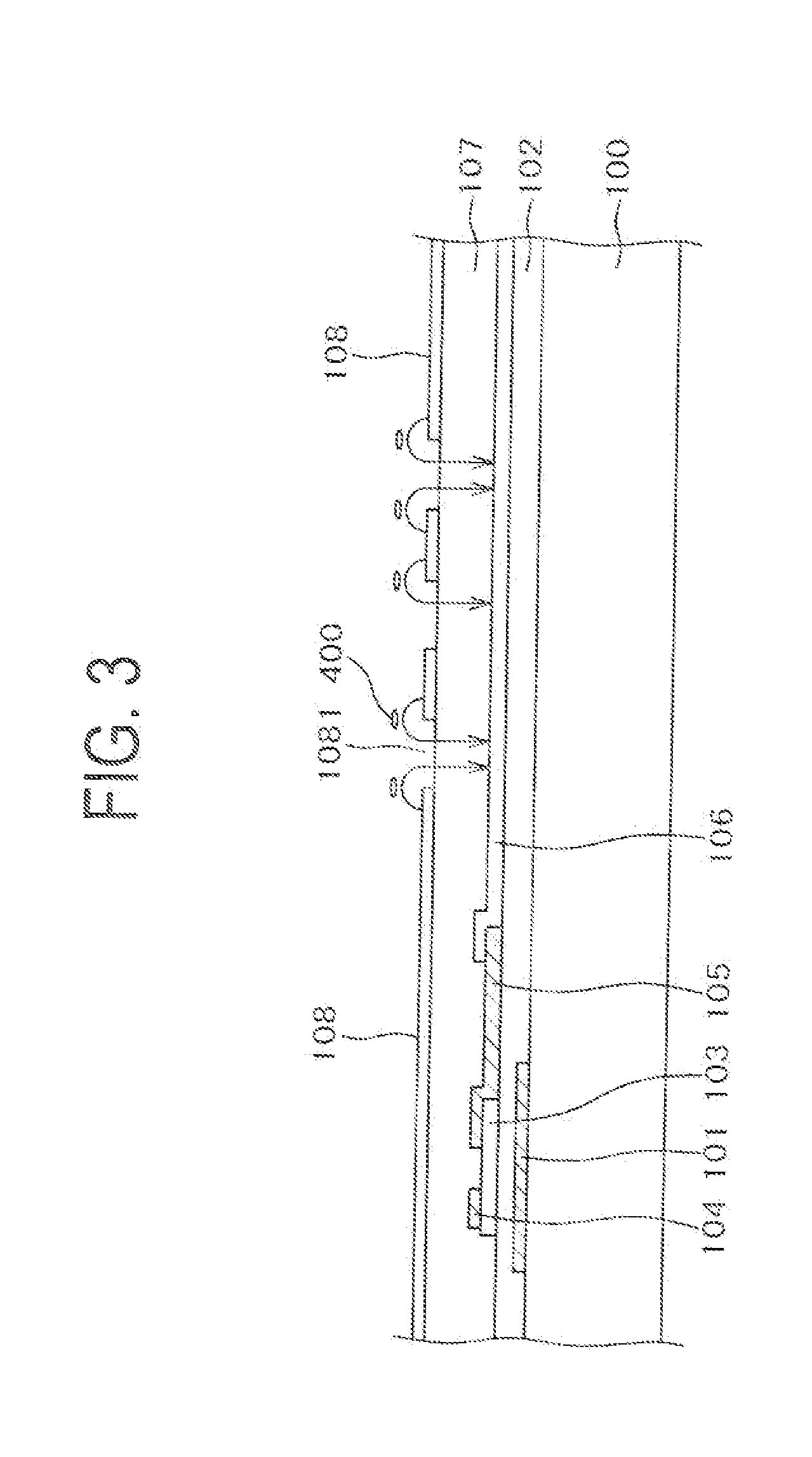
[0065]FIG. 11 is a cross-sectional view of the configuration for resistance adjustment in the straight wiring portion 33 in IPSLITE 1. In FIG. 11, the drain layer lead line 302 is used for the lead line 30. In FIG. 11, the drain layer lead line 302 is interrupted in the middle of the straight wiring portion 33, and the gap is connected with the bridging ITO. The bridging ITO is formed at the same time as the pixel electrode 106, namely, a lower ITO 50. In IPSLITE 1, the source electrode 105 is formed prior to the formation of the pixel electrode 106. Thus, in FIG. 11, the lower ITO 50 overlaps a portion of the drain layer lead line 302 to establish connection between them.

[0066]As described above, in this example, it is possible to adjust the resistance of the lead line 30 by the lower ITO 50, without using the through hole and the like. The resistance of the lead line 30 can be adjusted by the length of the lower ITO 50. Here, the number of process steps is not increased compared t...

second example

[0067]FIG. 12 is a cross-sectional view of the configuration for resistance adjustment in the straight wiring portion 33 in IPSLITE 2. In FIG. 12, the drain layer lead line 302 is used for the lead line 30. FIG. 12 is different from FIG. 11 in that the pixel electrode 106, namely, the lower ITO 50 is formed prior to the formation of the source electrode 105 in IPSLITE 2. Thus, the drain layer lead line 302 in FIG. 12 overlaps a portion, of the lower ITO 50 to ensure electrical continuity between the two electrodes. The other configuration and effect are the same as those in the first example.

third example

[0068]FIG. 13 is a cross-sectional view of the configuration for resistance adjustment in the straight wiring portion 33 in IPSLITE 3. In FIG. 13, the drain layer lead line 302 is used for the lead line 30. In FIG. 13, the pixel electrode 106, namely, the lower ITO 50 is used as the bridging ITO for the resistance adjustment. The resistance of the lead line 30 can be adjusted by the length of the lower ITO 50.

[0069]FIG. 13 is different from FIGS. 11 and 12 in that the lower ITO 50 is directly formed on the TFT substrate 100. Thus, a through hole is formed in the gate insulating film 102 to establish connection between the drain layer lead line 302 and the lower ITO 50 for the resistance adjustment. Of course, the lower ITO 50 below the gate insulating film 102 should be patterned and formed before the gate insulating film 102 is attached thereto. However, the patterning of the lower ITO 50 is performed at the same time as the patterning of the pixel electrode 106, so that the number...


PUM


Abstract

A drain layer lead line connecting an image signal line and a terminal of an IC driver is interrupted in the middle, and the gap is bridged by bridging ITO that is formed at the same time as pixel ITO. Thus, the difference in the length of the lead lines is adjusted such that the length of the bridging ITO in the lead line connected to the terminal in the center of the IC driver is longer than the length of the bridging ITO in the lead line connected to the terminal in the end of the IC driver to reduce the difference in the wiring resistance of the lead lines due to the difference in the length of the lead lines depending on the location.

Description

CLAIM OF PRIORITY[0001]The present application claims priority from Japanese Patent Application JP 2010-245416 filed on Nov. 1, 2011, the content of which is hereby incorporated by reference into this application.FIELD OF THE INVENTION[0002]The present invention relates to a display device, and more particularly, to a liquid crystal, display device designed to prevent uneven brightness due to wiring resistance.BACKGROUND OF THE INVENTION[0003]In a liquid crystal display panel used for a liquid crystal display device, there is provided a TFT substrate in which pixels each having a pixel electrode, a thin film transistor (TFT), and the like are arranged in a matrix form. There is also provided a counter substrate disposed opposite to the TFT substrate, in which color filters and the like are formed at positions corresponding to the pixel electrodes of the TFT substrate. Then, a liquid crystal is interposed between the TFT substrate and the counter substrate. Thus, an image is formed b...

Claims


Application Information

Patent Timeline
IPC IPC(8): G09G5/00G09G3/36
CPCG02F1/1345G02F1/1368G02F1/136286G02F1/13439
Inventor NAGAMI, TAKAHIRO
Owner JAPAN DISPLAY INC
Why Eureka
Try Eureka