Electroluminescence device having lead line with low resistance

a technology of electron microscopy and lead line, applied in the direction of luminescence screen, discharge tube, identification means, etc., can solve the problems of difficult to manufacture organic el devices, lowering image quality, adverse effects, etc., and achieve uniformity. the effect of resistan

Inactive Publication Date: 2005-06-16
SAMSUNG MOBILE DISPLAY CO LTD
View PDF10 Cites 16 Cited by
  • Summary
  • Abstract
  • Description
  • Claims
  • Application Information

AI Technical Summary

Benefits of technology

[0014] The present invention provides an organic electroluminescence (EL) device including a plurality of lines having widths corresponding to lengths thereof so that the different length lead lines may have uniform resistance.

Problems solved by technology

A desiccant is then injected into the organic OL device, and the device is sealed under a vacuum or nitrogen atmosphere, thereby increasing its durability, which is adversely affected by moisture and oxygen.
If the active area electrode lines have a high resistance, this may cause a voltage drop that generates a brightness difference between the 20 pixels, thereby lowering image quality.
Thus, it is difficult to manufacture the organic EL device, and the thicker lines may generate structural problems.
Therefore, the organic EL device's driving voltage and power consumption increase.

Method used


Image

  • Electroluminescence device having lead line with low resistance
  • Electroluminescence device having lead line with low resistance
  • Electroluminescence device having lead line with low resistance

Examples


Embodiment Construction

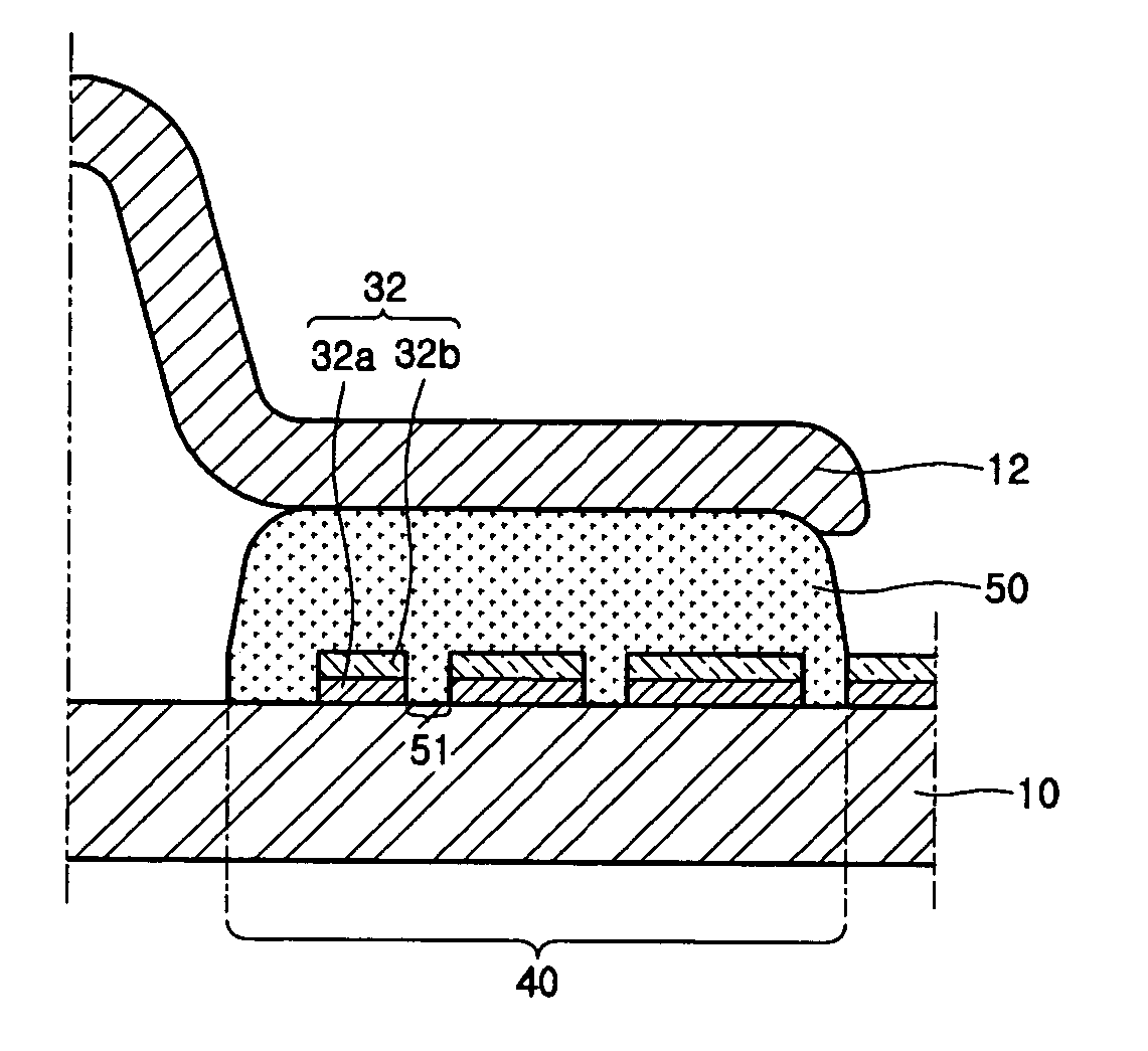
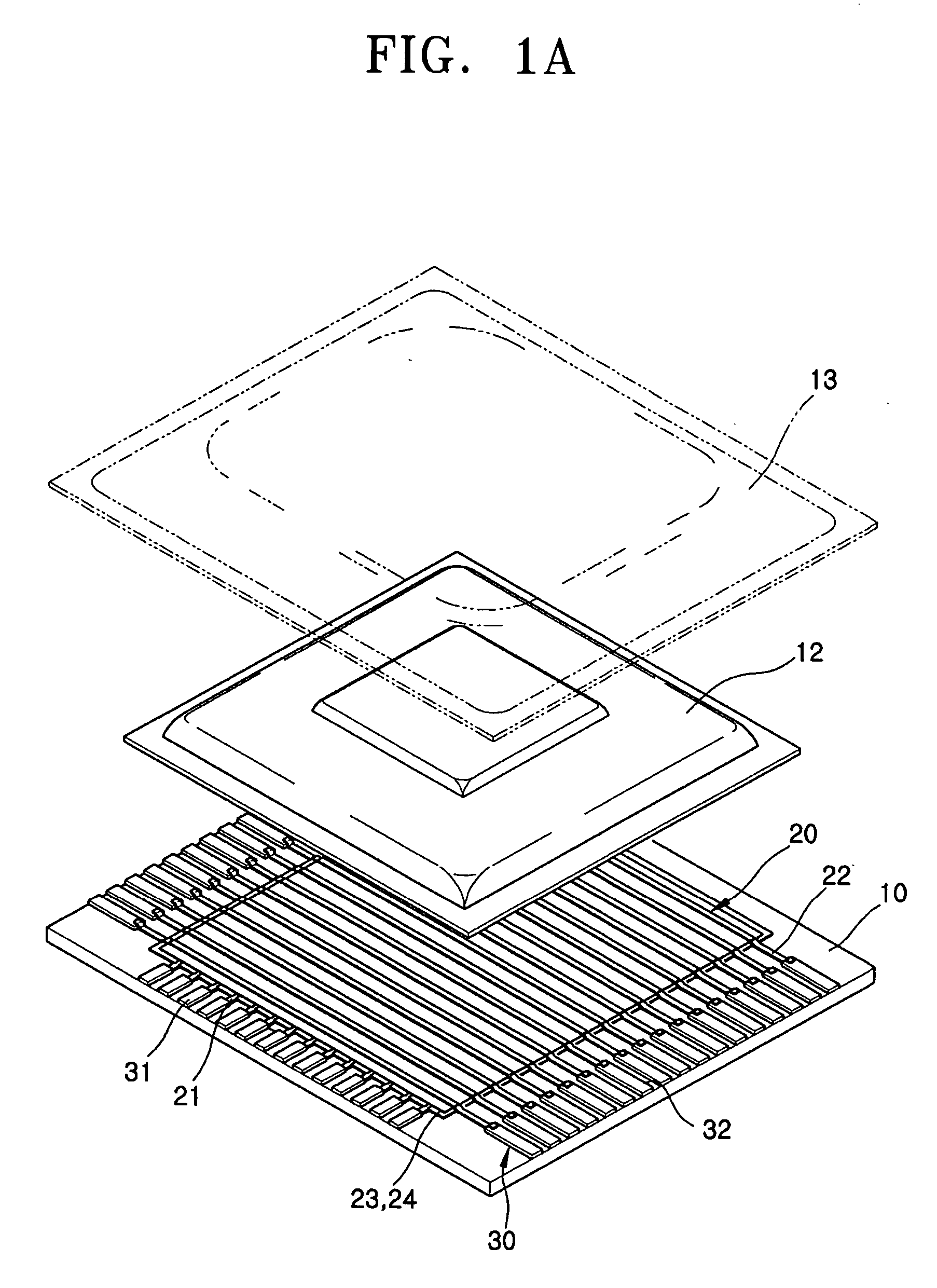
[0025]FIG. 2A is an exploded perspective view of a organic electroluminescence (EL) device according to an exemplary embodiment of the present invention and FIG. 2B is a plan view showing an enlarged part of the organic EL device of FIG. 2A. Referring to FIG. 2A and FIG. 2B, an organic EL device of this exemplary embodiment of the present invention includes a substrate 10, on which a plurality of electrodes (or electrode lines) forming an active area 20 are disposed. A cap 12 contains a desiccant and is sealed with the substrate 10 to prevent the active area 20 from being infiltrated by moisture, and a flexible printed circuit board (PCB) 13 connects the organic EL device to a circuit driving unit (not shown). The cap and substrate may be joined at area 40. A plurality of electrode lines include a plurality of first electrode lines 21 as positive electrodes and a plurality of second electrode lines 22 as negative electrodes. The first electrode lines 21 are connected to first lead l...


PUM


Abstract

An organic electroluminescence device including a plurality of electrodes formed on a substrate, and a plurality of lead lines are coupled to the plurality of electrodes. At least two or more lead lines among the plurality of lead lines have different widths, and a width of a longer lead line among the plural lead lines is greater than a width of a shorter lead line.

Description

[0001] This application claims the benefit of Korean Patent Application No. 2003-82635, filed on Nov. 20, 2003, which is hereby incorporated by reference for all purposes as if fully set forth herein. BACKGROUND OF THE INVENTION [0002] 1. Field of the Invention [0003] The present invention relates to an electroluminescence device, and more particularly, to an electroluminescence device having lead lines that are connected to a plurality of electrodes forming an electroluminescence unit, the lead lines having different widths corresponding to lengths thereof. [0004] 2. Discussion of the Related Art [0005] Many different types of display apparatuses are used to display images. Flat panel displays are replacing the conventional cathode ray tube (CRT) devices. Flat panel displays are either emissive type or non-emissive type depending upon how the panel emits light. A flat CRT, a plasma display panel device, a vacuum fluorescent display device, a field emission display device, and an el...

Claims


Application Information

Patent Timeline
Patent Type & Authority Applications(United States)
IPC IPC(8): G09F9/30H01L27/00H01L51/50H01L27/32H01L51/52H05B33/02H05B33/04H05B33/12H05B33/14H05B33/26H05B44/00
CPCH01L51/5237H01L27/3288H10K59/179H10K50/841H10K50/846H05B33/26
Inventor HEO, SE-JUNNAM, WI-JIN
Owner SAMSUNG MOBILE DISPLAY CO LTD
Why Eureka
Try Eureka