Light emitting device

a technology of light emitting element and discharge tube, which is applied in the direction of discharge tube/lamp details, discharge tube luminescnet screen, gas-filled discharge tube, etc., can solve the problems of unsuitable self-alignment performance, improper positioning of the mounted light emitting element, and the shape of the redundant reflow pad. , to achieve the effect of excellent self-alignment performance, excellent connection state and high quality

Active Publication Date: 2012-05-10
NICHIA CORP
View PDF5 Cites 24 Cited by
  • Summary
  • Abstract
  • Description
  • Claims
  • Application Information

AI Technical Summary

Benefits of technology

[0023]The light emitting device of the present invention has the following marked advantages.
[0024]The light emitting device with the first extended section and the second extended section prevents the reflowed heat-melted connecting material from generating solder balls while ensuring an excellent self-alignment performance. Therefore, the devices can be produced as high quality products, which are not affected by irregular alignments among the products generated in a mass assembly.
[0025]In particular, the light emitting device provided with the second extended section flanking the first extended sections prevents the reflowing heat-melted connecting material from converging towards the second substrate electrodes. Therefore, an excellent state of connection between the first substrate electrode and the first element electrode is attained.
[0026]The light emitting device further provided with a third extended section in the first substrate electrode can, after reflowing process, level the height of the elements, which are connected with each other by means of the heat-melted connecting material.
[0027]The light emitting device with the first extended section can, at the time of reflowing of the heat-melted material, prohibit the generation of solder balls while ensuring excellent self-alignment performance.

Problems solved by technology

Despite the above-mentioned prior art conventional light emitting devices have the following problems.
In the configuration of the light emitting device of patent document 1, the shape of the redundant reflow pad, which is formed to be larger than the electrode section of the element, is not suitable for self-alignment performance.
Therefore, improper self-alignment is a problem, which causes an improper positioning of the mounted light emitting element at the time of the reflowing process.
Therefore, when the device comprises separate die pads for one element such as a light emitting diode, in other words, when the configuration of the device comprises multiple electrodes on the side of a substrate, such as a first substrate electrode and a second substrate electrode mounted at separate positions on the substrate, the configuration is unsatisfactory for performing self-alignment while preventing the solder ball generation.
Therefore, the converging molten solder forms an excessive connecting thickness of the second electrode, and may lift up some portion of the molten solder around the first electrode, generating voids in the molten solder near the first electrode.

Method used


Image

  • Light emitting device
  • Light emitting device
  • Light emitting device

Examples


Embodiment Construction

[0038]In the following sections, embodiments of the light emitting device of the present invention are described with reference to the figures.

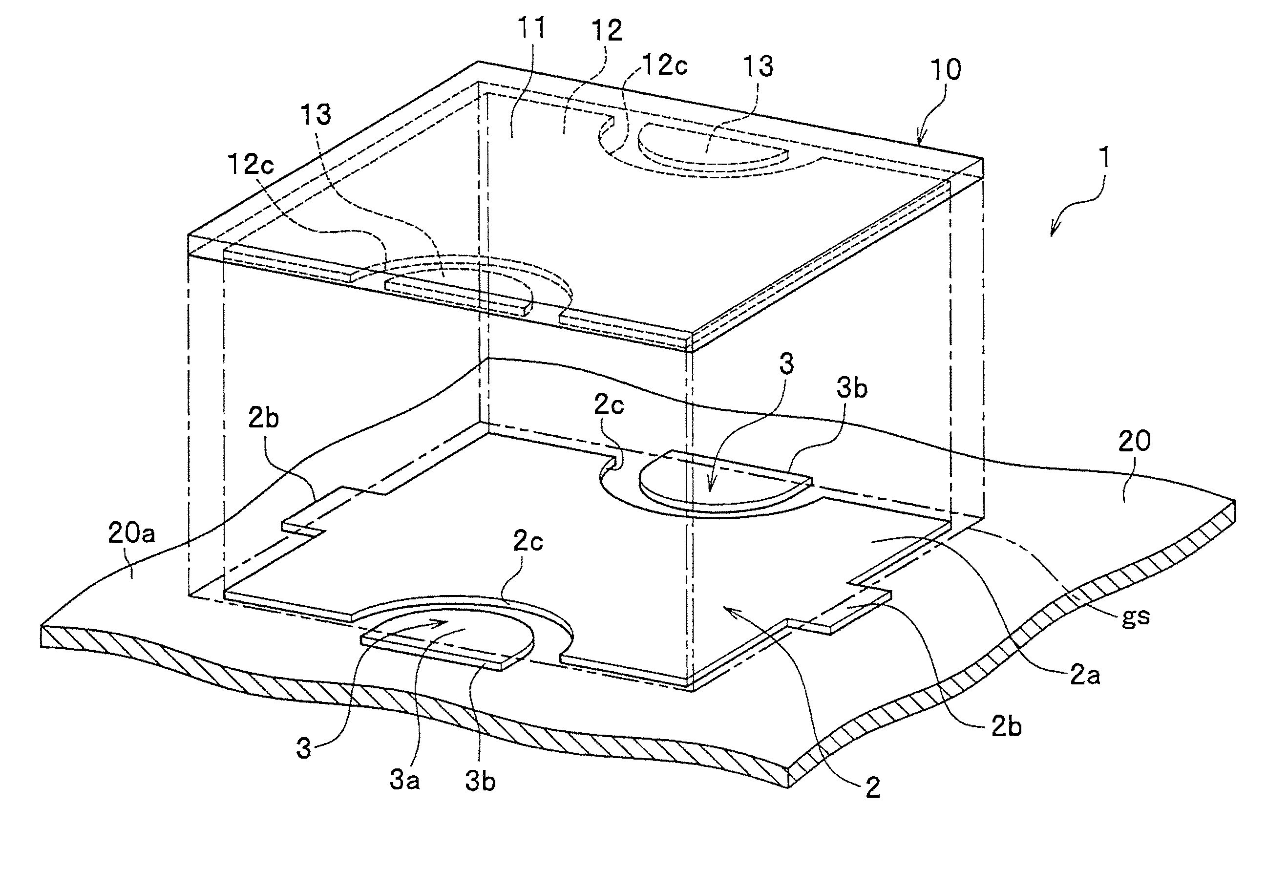
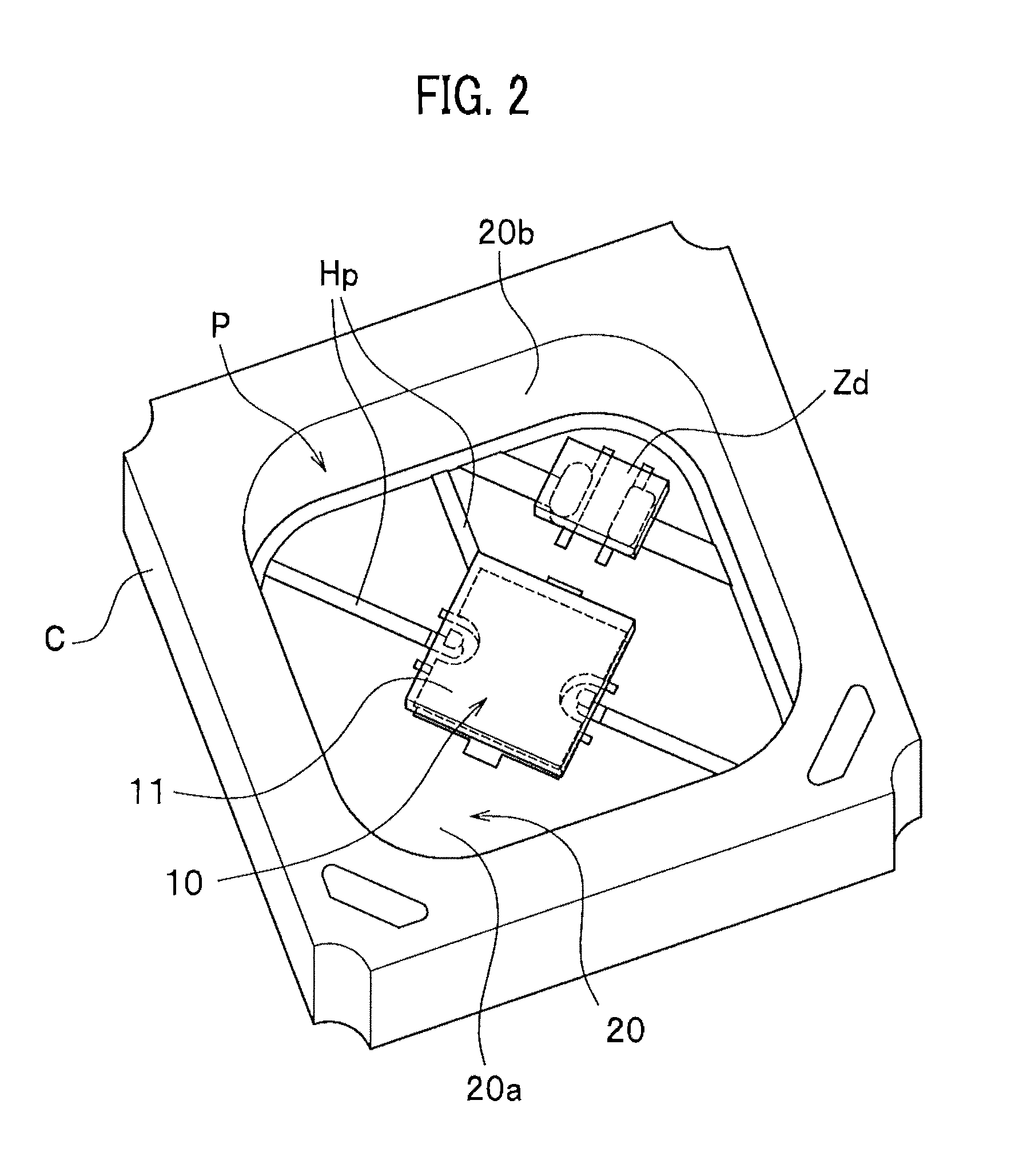
[0039]As shown in FIGS. 1 and 2, the light emitting device 1 is provided with a mounting substrate 20 formed to have a recessed portion in its center, and with a light emitting element (an element) 10, such as a LED chip, mounted on the central recessed portion of the mounting substrate 20. One example of the light emitting device 1 has a configuration comprising: a case C encompassing the recessed portion formed in the center of the mounting substrate 20; a wiring pattern Hp formed on the substrate's top face 20a where the light emitting element 10 is to be mounted in the center; the light emitting element 10 electrically connected, via an applied heat-melted connecting material kh such as solder paste, to the substrate electrodes (such as the first substrate electrode 2 and the second substrate electrodes 3) continuously connected to the wi...


PUM


Abstract

Disclosed is a light emitting device (1) comprising a rectangular element (10) mounted upon a mounting substrate (20) via a heat-melted connecting material, wherein second substrate electrodes (3) are formed conforming to the recesses (2c) of a first substrate electrode (2) and a portion of the outer periphery of the first and second substrate electrodes (2,3) is provided with first extended sections (2b) that extend farther outward than the outer periphery (gs) of the aforementioned element (10). The aforementioned first extended sections (2b) are formed in at least one or more locations per one side of the outer periphery (gs) of the aforementioned rectangular element (10); the aforementioned first substrate electrode (2) is provided with second extended sections (2d) that are formed on at least one of both ends of the aforementioned recesses (2c) flanking the first extended sections (2b) of the aforementioned second substrate electrodes; and the aforementioned second extended sections (2b) extend farther outward than the outer periphery of the aforementioned element (gs).

Description

FIELD OF THE INVENTION[0001]The present invention relates to a light emitting device, in which elements such as light emitting elements are mounted on a mounting substrate such as a semiconductor insulating substrate.BACKGROUND[0002]A surface-mounting type light emitting device with a light emitting element such as a light emission diode (LED) or a laser diode (LD) mounted on a substrate is conventionally well known. The light-emitting device has been used in lighting equipment, a backlight for display screen, an automotive illuminant, a display illuminant, and an auxiliary illuminant for motion pictures, as well as for other general consumer illuminants. In those applications, a device with a configuration comprising both anodes and cathodes mounted on the same surface is widely used in order to enhance its light extraction efficiency. A widely proposed light-emitting device has a configuration comprising chips mounted, by a flip-chip method, on an insulating substrate, on which wi...

Claims


Application Information

Patent Timeline
Patent Type & Authority Applications(United States)
IPC IPC(8): H01J1/88
CPCH01L24/05H01L2224/32225H01L24/29H01L24/32H01L24/83H01L33/38H01L33/62H01L2224/04026H01L2224/16H01L2224/83192H01L2224/83194H01L2224/83801H01L2924/01004H01L2924/01013H01L2924/01033H01L2924/01038H01L2924/01056H01L2924/01058H01L2924/01063H01L2924/01078H01L2924/01079H01L2924/01082H01L2924/014H01L2924/00013H01L2924/01005H01L2924/01006H01L2924/01047H01L2924/12041H01L2224/05599H01L2224/0556H01L2224/06051H01L2224/05552H01L2224/0401H01L24/06H01L2224/13099H01L2224/05099H01L2224/13599H01L2224/29099H01L2224/29599H01L2924/3512H01L2924/00H01L2924/00012H01L2924/12035H01L2924/12042H01L23/12H01L33/48
Inventor SUZUKI, RYOHAYASHI, TADAOTSUKIOKA, TOMOYATAKEUCHI, YOSHIKAZU
Owner NICHIA CORP
Why Eureka
Try Eureka