Display panel apparatus and method of fabricating display panel apparatus
- Summary
- Abstract
- Description
- Claims
- Application Information
AI Technical Summary
Benefits of technology
Problems solved by technology
Method used
Image

Examples
embodiment 1
[0083]The following shall describe the display panel apparatus according to Embodiment 1 of the present invention with reference to the drawings.
[0084](Overview of the Display Panel Apparatus)
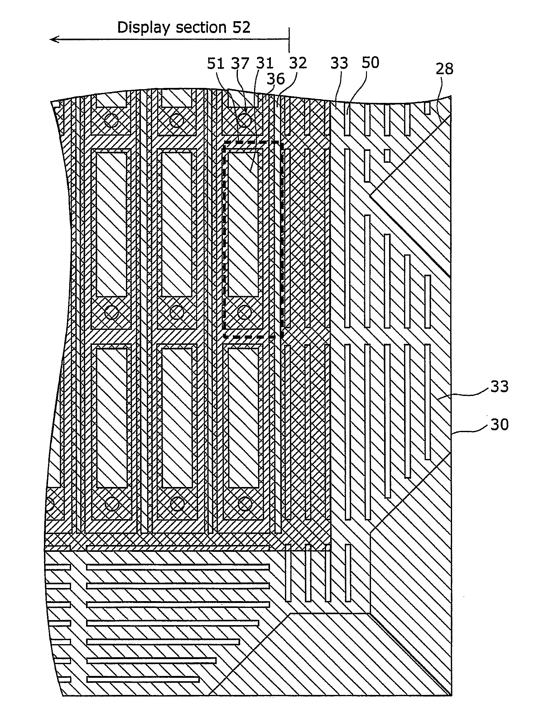
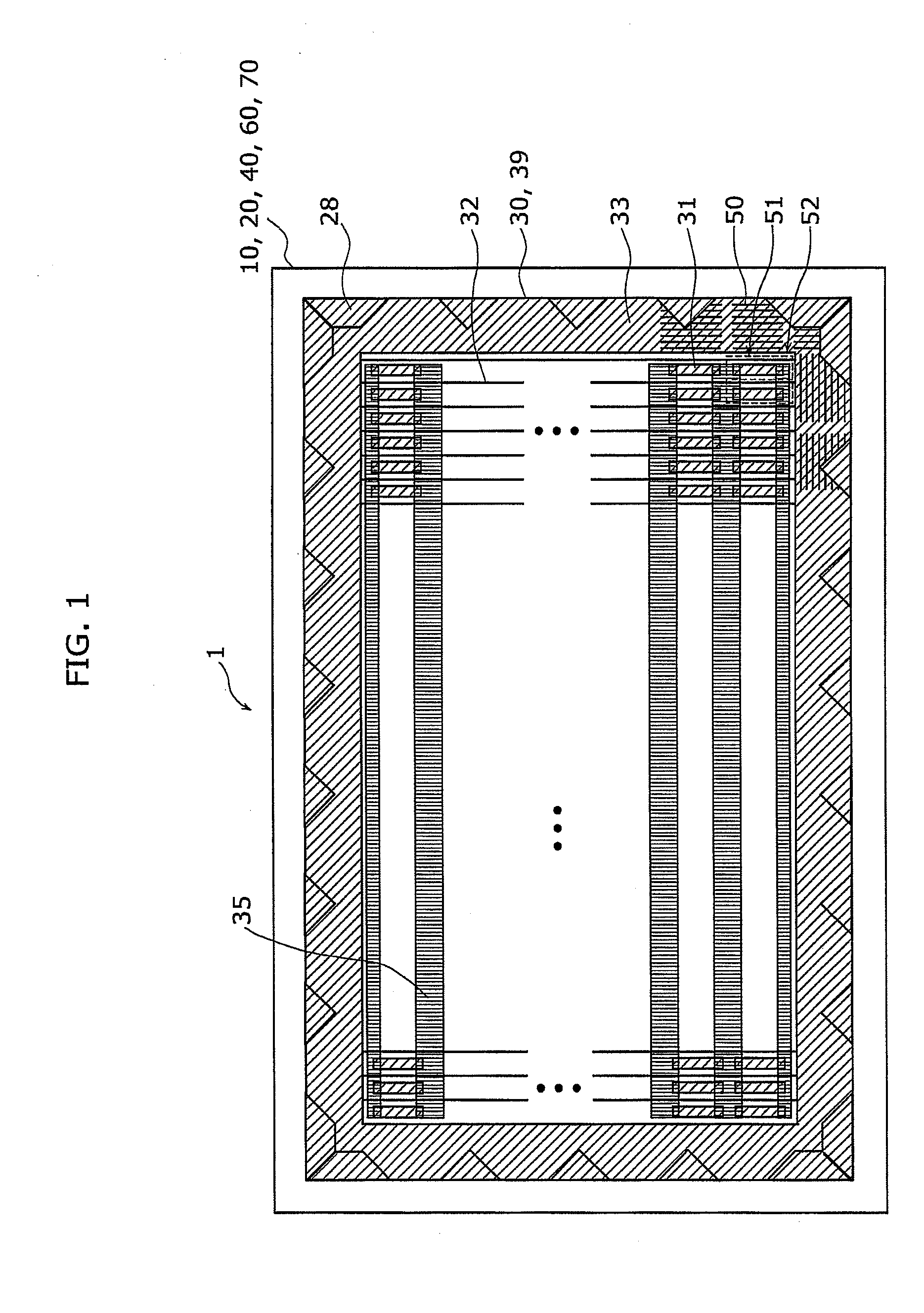
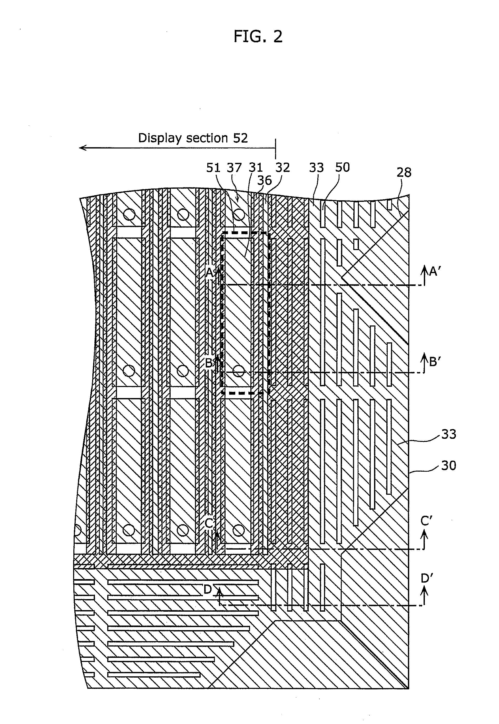
[0085]FIG. 1 is a planar view illustrating an example of the configuration of the display panel apparatus according to Embodiment 1 of the present invention.
[0086]As illustrated in FIG. 1, the display panel apparatus 1 is configured with a stacked structure including a TFT layer 20 and a planarizing film 30 stacked on a substrate 10 in this order, a display section 52 provided with the arranged pixels 51 which can be individually controlled for light emission, and a sealing film 40, a resin layer 60, and a glass substrate 70 sealing the entire surface.
[0087]The display section 52 includes pixels 51 arranged in a matrix. The pixels 51 include the organic EL device having lower electrodes 31 separated for each pixel 51, an upper electrode 39 provided on the entire surface and shared by all of the...
embodiment 2
[0181]Next, the display panel apparatus 2 according to Embodiment 2 of the present invention shall be described with reference to the drawings. Note that, the same reference numerals are assigned to the components with the same function as the components in the display panel apparatus 1 according to Embodiment 1, and the description for these components is simplified or omitted.
[0182]The display panel apparatus 2 according to Embodiment 2 of the present invention is different from the display panel apparatus 1 according to Embodiment 1 in that the configuration of the electrode plate 33 covers the holes 50. More specifically, in the display panel apparatus 1 according to Embodiment 1 of the present invention, the holes 50 are covered by extending a part of the hole injection layer 34 made of inorganic material. In contrast, in the display panel apparatus 2 according to Embodiment 2 of the present invention, a part of the pixel regulating layer 35 made of inorganic material is extend...
embodiment 3
[0230]Next, the display panel apparatus 3 according to Embodiment 3 of the present invention shall be described with reference to the drawings. Note that, the same reference numerals are assigned to the components with the same function as the components in the display panel apparatuses 1 and 2 according to Embodiments 1 and 2, and the description for these components are simplified or omitted.
[0231]The display panel apparatus 3 according to Embodiment 3 of the present invention is different from the display panel apparatuses 1 and 2 according to Embodiments 1 and 2 in that the configuration of the electrode plate 33 covers the holes 50. More specifically, in the display panel apparatuses 1 and 2 according to Embodiments 1 and 2 of the present invention, the holes 50 are covered by extending either a part of the hole injection layer 34 or the pixel regulating layer 35 made of inorganic material. In contrast, in the display panel apparatus 3 according to Embodiment 3 of the present i...
PUM
 Abstract
Description
Claims
Application Information
 - Generate Ideas
- Intellectual Property
- Life Sciences
- Materials
- Tech Scout
- Unparalleled Data Quality
- Higher Quality Content
- 60% Fewer Hallucinations
Browse by: Latest US Patents, China's latest patents, Technical Efficacy Thesaurus, Application Domain, Technology Topic, Popular Technical Reports.
© 2025 PatSnap. All rights reserved.Legal|Privacy policy|Modern Slavery Act Transparency Statement|Sitemap|About US| Contact US: help@patsnap.com