Compound semiconductor device having insulation film with different film thicknesses beneath electrodes

a semiconductor device and film thickness technology, applied in the field of compound semiconductor devices having filed plate electrodes, can solve the problems of reducing the effect of electric field concentration due to a conventional field plate electrod

Active Publication Date: 2012-05-24
SANKEN ELECTRIC CO LTD
View PDF20 Cites 47 Cited by
  • Summary
  • Abstract
  • Description
  • Claims
  • Application Information

AI Technical Summary

Problems solved by technology

In this case, however, a problem arose that an effect to alleviate electric

Method used


Image

  • Compound semiconductor device having insulation film with different film thicknesses beneath electrodes
  • Compound semiconductor device having insulation film with different film thicknesses beneath electrodes
  • Compound semiconductor device having insulation film with different film thicknesses beneath electrodes

Examples


first embodiment

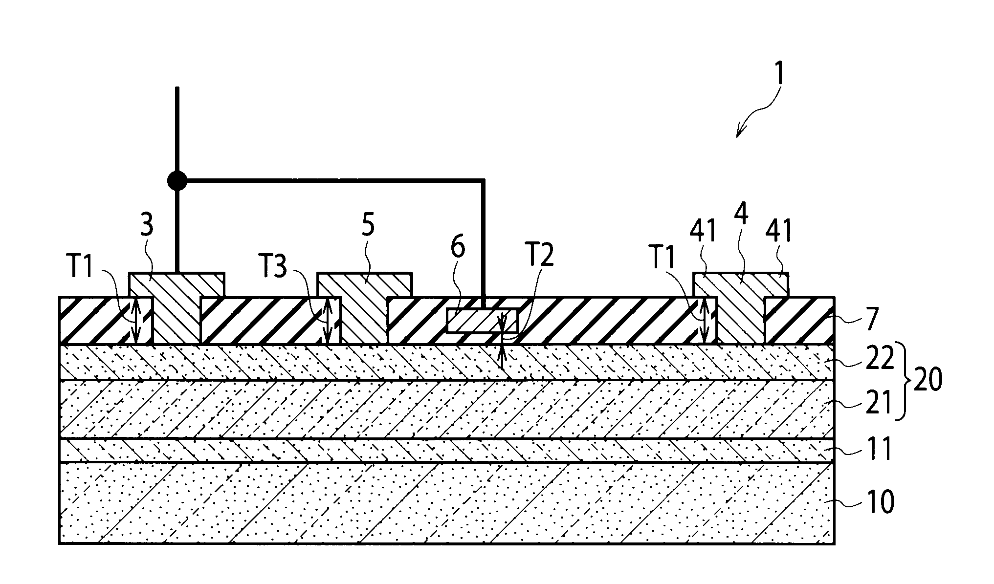
[0020]As illustrated in FIG.1, a compound semiconductor device 1 according to the first embodiment of the present invention includes a group-III nitride semiconductor layer 20 in which a carrier supply layer 22 and a carrier travel layer 21 which forms a hetero j unction with the carrier supply layer 22 are laminated, an insulation film 7 located on the group-III nitride semiconductor layer 20, a source electrode 3, a drain electrode 4, and a gate electrode 5. The drain electrode 4 is located at a position which is a first distance T1 away from the top surface of the group-III nitride semiconductor layer 20 in the film thickness direction through the insulation film 7. The source electrode 3 is located at a position which is the first distance T1 away from the top surface of the group-III nitride semiconductor layer 20 in the film-thickness direction through the insulation film 7. The gate electrode 5 is located between the source electrode 3 and the drain electrode 4 at a position ...

second embodiment

[0053]As illustrated in FIG. 13, a compound semiconductor device 1 according to the second embodiment of the present invention is different from the compound semiconductor device 1 shown in FIG. 1 in that a shield electrode 8 is further provided on a group-III nitride semiconductor layer 20 between and in the adjacent to a gate electrode 5 and a field plate electrode 6. As seen in FIG. 13, the shield electrode 8 is electrically connected to the field plate electrode 6. Also, the shield electrode 8 and the field plate electrode 6 are electrically connected to a source electrode 3. The rest of the structure is similar to the first embodiment illustrated in FIG. 1.

[0054]The structure of the shield electrode 8 may be similar to that of, for example, the gate electrode 5. FIG. 13 shows an example where the outer edge portion of the shield electrode 8 is located on an insulation film 7 so that the shield electrode 8 has a flange portion. However, the shield electrode 8 does not necessaril...


PUM


Abstract

A compound semiconductor device includes a group-III nitride semiconductor layer; an insulation film located on the group-III nitride semiconductor layer; a drain electrode located in a position which is a first distance away from an upper surface of the group-III nitride semiconductor layer; a source electrode located in a position which is the first distance away from the upper surface of the group-III nitride semiconductor layer; a gate electrode located between the drain electrode and the source electrode; and a field plate electrode located between the drain electrode and the gate electrode at a position which is a second distance away from the upper surface of the group-III nitride semiconductor layer, the second distance is shorter than the first distance.

Description

CROSS REFERENCE TO RELATED APPLICATIONS AND INCORPORATION BY REFERENCE[0001]This application is based upon and claims the benefit of priority from prior Japanese Patent Application P2010-258799 filed on Nov. 19, 2010; the entire contents of which are incorporated by reference herein.[0002]10BACKGROUND OF THE INVENTION[0003]1. Field of the Invention[0004]The present invention relates to a compound semiconductor device having a filed plate electrode.[0005]2. Description of the Related Art[0006]A compound semiconductor device using a group-III nitride semiconductor is used for a high-voltage power device and the like. Atypical group-III nitride semiconductor is expressed as AlxInyGa1-x-yN (0< / =x< / =1, 0< / =y< / =1, 0< / =x+y< / =1), and includes gallium nitride (GaN), aluminum nitride (AlN), and indium nitride (InN). For example, for a high-electron-mobility transistor (HEMT), a hetero junction surface is formed in an interface between a carrier travel layer and a carrier sup...

Claims


Application Information

Patent Timeline
IPC IPC(8): H01L29/772
CPCH01L29/2003H01L29/402H01L29/7787H01L29/66462H01L29/41725H01L29/0619
Inventor AOKI, HIRONORI
Owner SANKEN ELECTRIC CO LTD
Why Eureka
Try Eureka