Method and apparatus for fabricating crack-free Group III nitride semiconductor materials

a technology of nitride and semiconductor materials, applied in the field of semiconductor materials, can solve the problems of limiting their performance as well as their commercial viability, their tendency to crack, and even forming cracks on the substra

Inactive Publication Date: 2005-06-30
FREIBERGER COMPOUND MATERIALS
View PDF57 Cites 233 Cited by
  • Summary
  • Abstract
  • Description
  • Claims
  • Application Information

AI Technical Summary

Benefits of technology

[0006] The present invention provides a method and apparatus for growing low defect, optically transparent, colorless, crack-free single crystal Group III nitride epitaxial layers with a thickness exceeding 10 microns. These layers can be grown on large area substrates. Suitable substrate materials include silicon (Si), silicon carbide (SiC), sapphire, gallium nitride (GaN), aluminum nitride (AlN), gallium arsenide (GaAs), aluminum gallium nitride (AlGaN) and others.

Problems solved by technology

Unfortunately, these materials suffer from a variety of problems that limit their performance as well as their commercial viability.
One of the principal problems associated with Group III nitride materials is their tendency to crack, a problem that has been described in numerous scientific papers.
Occasionally cracks even form in the substrate on which the layer is being grown.

Method used


Image

  • Method and apparatus for fabricating crack-free Group III nitride semiconductor materials
  • Method and apparatus for fabricating crack-free Group III nitride semiconductor materials
  • Method and apparatus for fabricating crack-free Group III nitride semiconductor materials

Examples


embodiments

Embodiment 1

AlN Material Growth and Wafer Preparation

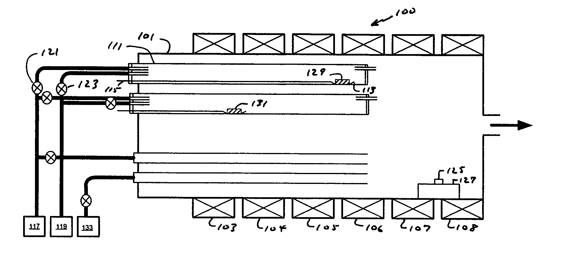
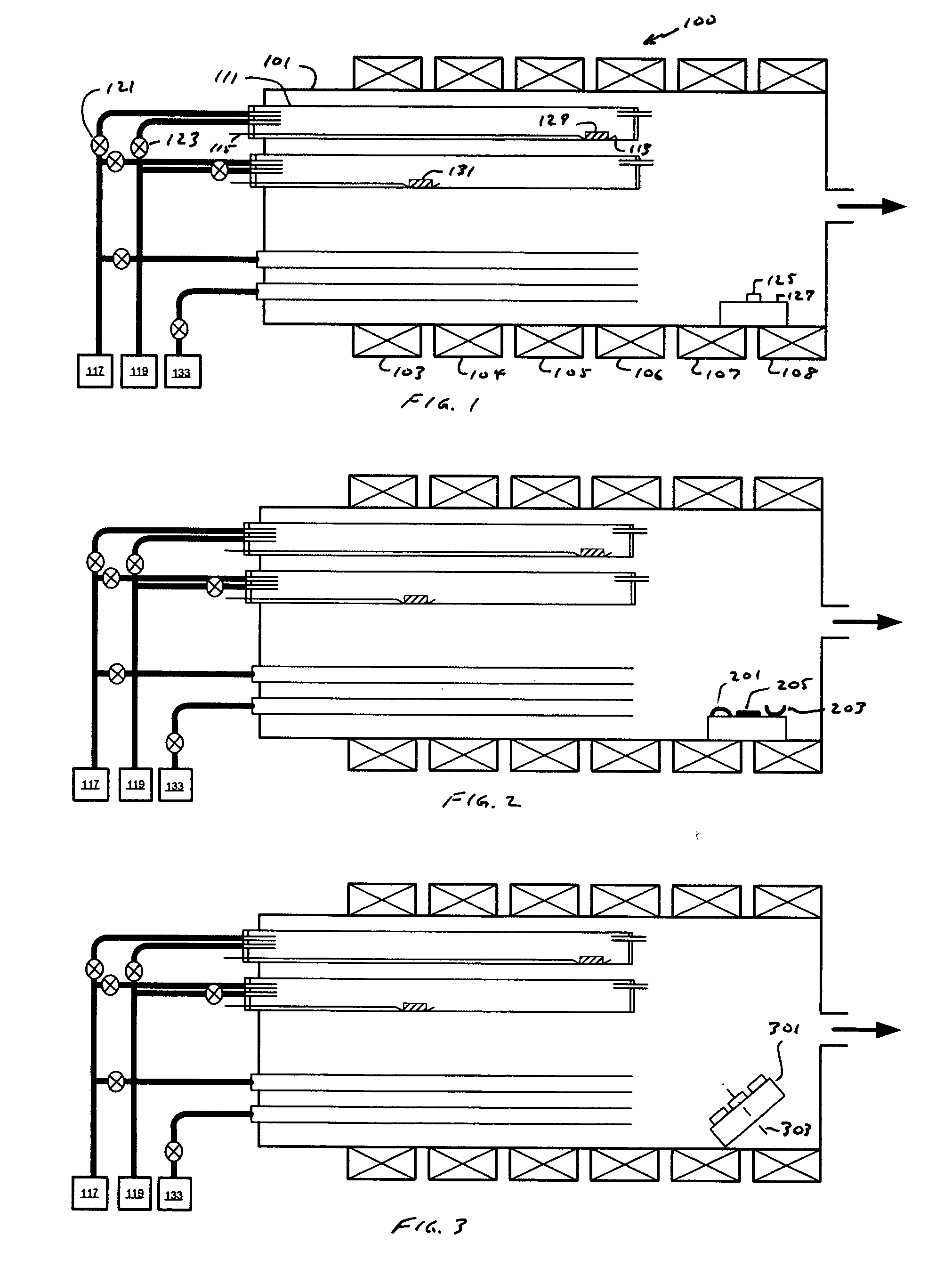
[0066] The growth of AlN material by the inventive process was performed in an inert gas flow at atmospheric pressure in a hot-wall, horizontal reactor chamber. SiC substrates were placed on a quartz pedestal and loaded into the growth zone of the quartz reactor. The growth was performed on the (0001)Si on-axis 6H-SiC substrate, the substrates having a surface rms roughness of approximately 0.3 nm or better.

[0067] Approximately 1 pound of Al metal (5N) was placed in a sapphire source boat for use in growing the AlN thick layer. For extended runs, typically those requiring a growth cycle of more than 48 hours, multiple Al sources / boats were used, either in parallel or sequentially. The source boat was placed in a quartz source tube (i.e., source channel) within the source zone of the reactor. This source tube (or tubes when multiple Al sources were used) supplied AlCl3 to the growth zone of the reactor. Additional quartz tubes (...

embodiment 2

AlN Material Growth and Wafer Preparation

[0072] Using a modified HVPE process, a 400 micron thick AlN boule was grown on a 2 inch SiC substrate at a growth temperature of 900° C. and at a growth rate of 30 microns per hour. The AlN boule was grown in the growth sub-zone yielding substantially flat layer growth. After completion of the growth cycle, the SiC substrate was removed by a combination of chemical etching, RIE and mechanical polishing. The resultant AlN wafer was polished, etched and cleaned and then re-introduced into the flat growth sub-zone of the HVPE reactor. A 1 centimeter thick AlN boule was grown on the (0001)N face of the prepared AlN seed wafer, the resultant boule being crack-free.

[0073] The AlN boule was sliced into 8, 2-inch AlN wafers with thicknesses ranging from 200 to 500 microns. X-ray diffraction studies showed that the AlN wafers had a single crystal structure (e.g., the FWHM of the x-ray RC was less than 300 arc sec).

[0074] The AlN wafers were subjec...

embodiment 3

AlN Device Fabrication

[0075] The growth of AlN material by the inventive process was performed in an inert gas flow at atmospheric pressure in a hot-wall, horizontal reactor chamber. Two inch SiC substrates were placed on a quartz pedestal and loaded into the growth zone of the quartz reactor, positioned for AlN deposition on the (0001) Si on-axis surface.

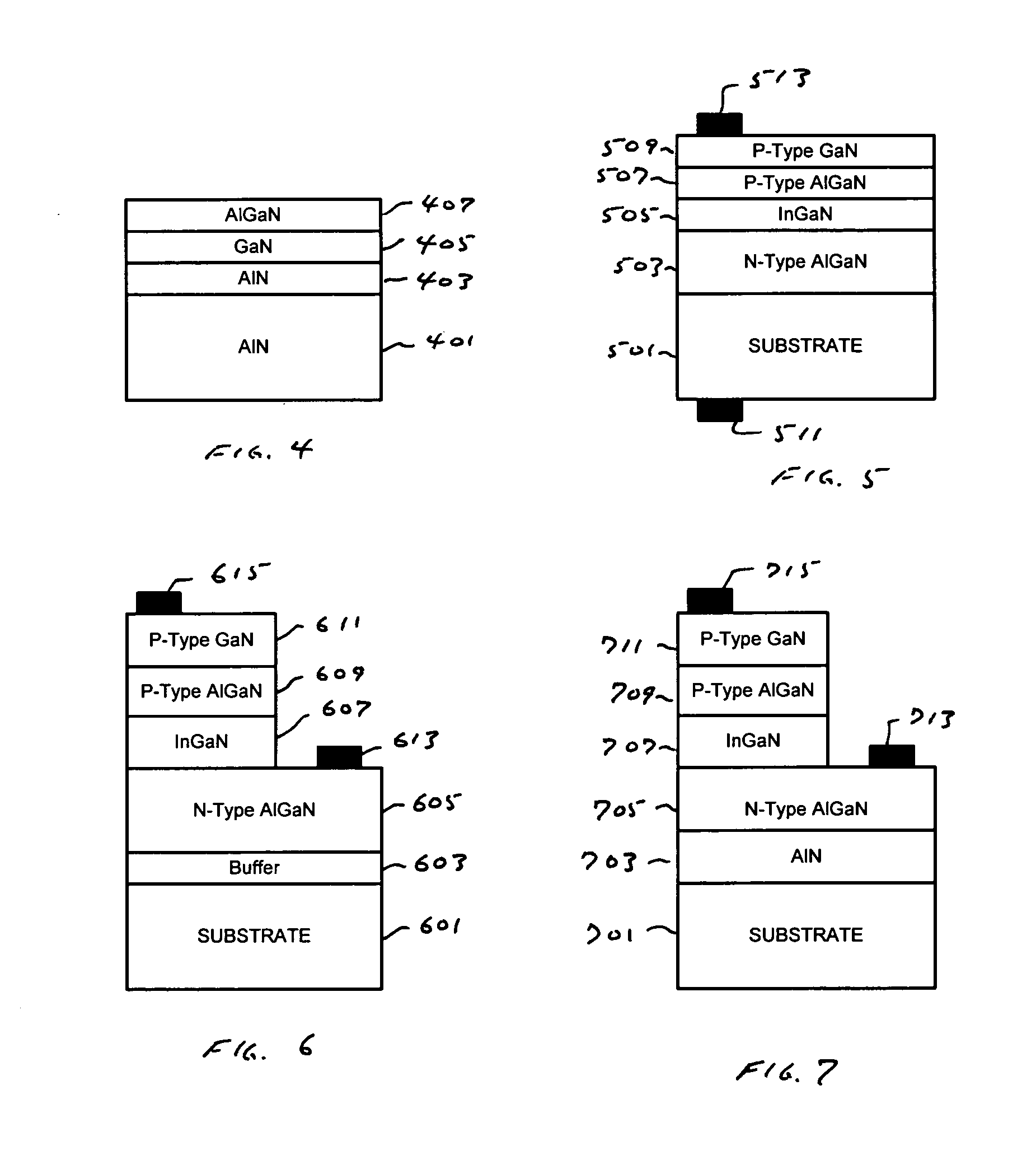
[0076] Approximately 1 kilogram of Al metal was placed in the source boat. After purging the reactor with Ar gas, the growth zone and the Al source zone were heated to 920° C. and 750° C., respectively. To prepare the substrates for AlN deposition, HCl gas was introduced into the growth zone to etch the SiC substrates. The HCl gas was then introduced into the Al source zone, thereby forming aluminum chloride that was transported into the growth zone by the Ar carrier gas. Simultaneously, NH3 gas was introduced into the growth zone, the NH3 gas providing a source of nitrogen. As a result of the reaction between the aluminum chlori...


PUM

PropertyMeasurementUnit
temperatureaaaaaaaaaa
thickaaaaaaaaaa

Abstract

A method and apparatus for growing low defect, optically transparent, colorless, crack-free, substantially flat, single crystal Group III nitride epitaxial layers with a thickness of at least 10 microns is provided. These layers can be grown on large area substrates comprised of Si, SiC, sapphire, GaN, AlN, GaAs, AlGaN and others. In one aspect, the crack-free Group III nitride layers are grown using a modified HVPE technique. If desired, the shape and the stress of Group III nitride layers can be controlled, thus allowing concave, convex and flat layers to be controllably grown. After the growth of the Group III nitride layer is complete, the substrate can be removed and the freestanding Group III nitride layer used as a seed for the growth of a boule of Group III nitride material. The boule can be sliced into individual wafers for use in the fabrication of a variety of semiconductor structures (e.g., HEMTs, LEDs, etc.).

Description

PRIORITY CLAIM [0001] The present application claims benefit of the filing date of U.S. Provisional Patent Application Ser. No. 60 / 449,085, filed Feb. 21, 2003 and is a continuation-in-part application of U.S. patent application Ser. No. 10 / 355,426, filed Jan. 31, 2003 which is a continuation-in-part of U.S. patent application Ser. No. 09 / 900,833, filed Jan. 6, 2001, now U.S. Pat. No. 6,613,143, and of U.S. patent application Ser. No. 09 / 903,047, filed Jul. 11, 2001, which is a continuation-in-part of U.S. patent application Ser. No. 09 / 900,833, filed Jan. 6, 2001, now U.S. Pat. No. 6,613,143, and of U.S. patent application Ser. No. 10 / 632,736, filed Aug. 1, 2003, which is a continuation of U.S. patent application Ser. No. 09 / 903,047, filed Jul. 11, 2001, which is a continuation-in-part of U.S. patent application Ser. No. 09 / 900,833, filed Jan. 6, 2001, now U.S. Pat. No. 6,613,143; the disclosures of all of the cited applications and patents are incorporated herein for any and all p...

Claims


Application Information

Patent Timeline
Patent Type & Authority Applications(United States)
IPC IPC(8): C30B25/00
CPCC30B25/00C30B29/403C30B25/02Y10S117/915Y10T428/21
Inventor DMITRIEV, VLADIMIR A.MELNIK, YURI V.
Owner FREIBERGER COMPOUND MATERIALS
Why Eureka
Try Eureka