
Thin film deposition method of nitride semiconductor and nitride semiconductor light emitting device

a technology of nitride and light-emitting devices, which is applied in semiconductor devices, lasers, semiconductor lasers, etc., can solve the problems of increasing the laser oscillation threshold value and operation power consumption, preventing the characteristic improvement of light-emitting devices using nitride, and no suitable metallic material with a work function enabling good ohmic contact, etc., to suppress the loss of internal quantum efficiency and reduce the adverse effect of contact resistan

Inactive Publication Date: 2005-07-19
NIPPON TELEGRAPH & TELEPHONE CORP
View PDF10 Cites 230 Cited by
  • Summary
  • Abstract
  • Description
  • Claims
  • Application Information

AI Technical Summary

Benefits of technology

[0010]The present invention provides a technique to reduce the adverse effect the contact resistance between the p-type nitride semiconductor and electrode, which causes a problem in the light emitting devices such as light emitting diodes and semiconductor lasers using nitride semiconductors, can have on the device characteristics, and a technique to suppress the loss of the internal quantum efficiency of the injected carriers due to the nonradiative surface recombination, which causes a problem in nitride semiconductor lasers. An object of the present invention is to provide a nitride semiconductor light emitting device and a thin film deposition method for the device capable of solving the foregoing two problems simultaneously.
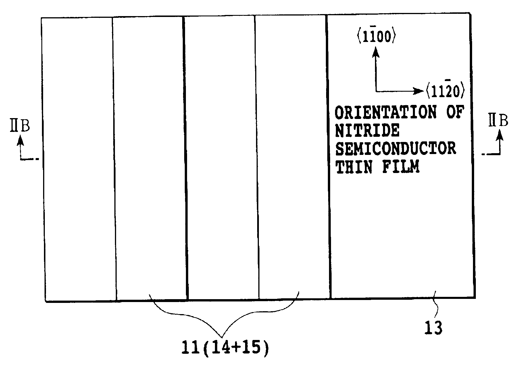
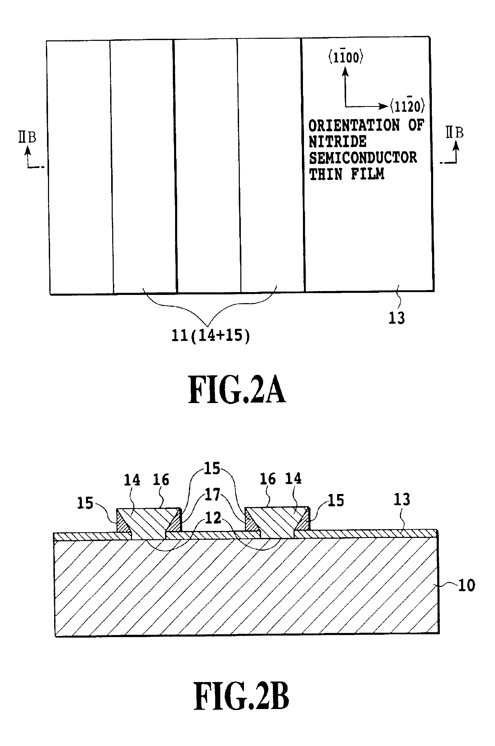
[0012]The nitride semiconductor thin films (A+B) formed in this method are composed of the p-type low resistance portion (A) formed as a result of the growth of the (0001) plane and the high resistance portion (B) formed as a result of the growth of the {11−2x} facets (x=0, 1, 2). Thus, a p-type contact layer is obtained which operates as a current confinement layer of the nitride semiconductor light emitting device. This makes it possible to increase the area of a p-type electrode as compared with that of the conventional devices, and to reduce the loss of power due to contact resistance.
[0013]In addition, when forming in advance on a principal orientation plane of the substrate a stripe-like nitride semiconductor base layer that is parallel to a [1-100] direction of a nitride semiconductor to be grown by selective-area growth and has a (0001) plane as a principal orientation plane, or a polygon-like nitride semiconductor base layer whose side is parallel to a [1-100] direction of nitride semiconductors to be grown by selective-area growth and which has a (0001) plane as a principal orientation plane; growing nitride semiconductor thin films on the principal orientation plane and side facets of the nitride semiconductor base layer by selective-area growth by vapor phase growth using a gas containing metallic magnesium or magnesium compound, the nitride semiconductor thin films (A+B) being composed of a first nitride semiconductor crystal portion (A) formed as a result of growth in the direction perpendicular to the (0001) principal plane and a second nitride semiconductor crystal portion (B) formed as a result of growth of {11−2x} (x=0, 1, 2) facets; and making Mg concentration of the second nitride semiconductor crystal portion (B) lower than that of the first nitride semiconductor crystal portion (A), the nitride semiconductor thin films (A+B) formed in this method are composed of the p-type low resistance portion (A) formed as a result of the growth of the (0001) plane and the high resistance portion (B) formed as a result of the {11−2x} facets (x=0, 1, 2). Thus, a p-type contact layer is obtained which operates as a current confinement layer of the nitride semiconductor light emitting device. This makes it possible to increase the area of a p-type electrode as compared with that of the conventional devices, and to reduce the loss of power due to contact resistance. In addition, since the nitride semiconductor thin films are usable for the cladding layer of an index-guided nitride semiconductor laser, the nonradiative surface recombination of injected carriers can be suppressed, thereby reducing the oscillation threshold value of the laser.

Problems solved by technology

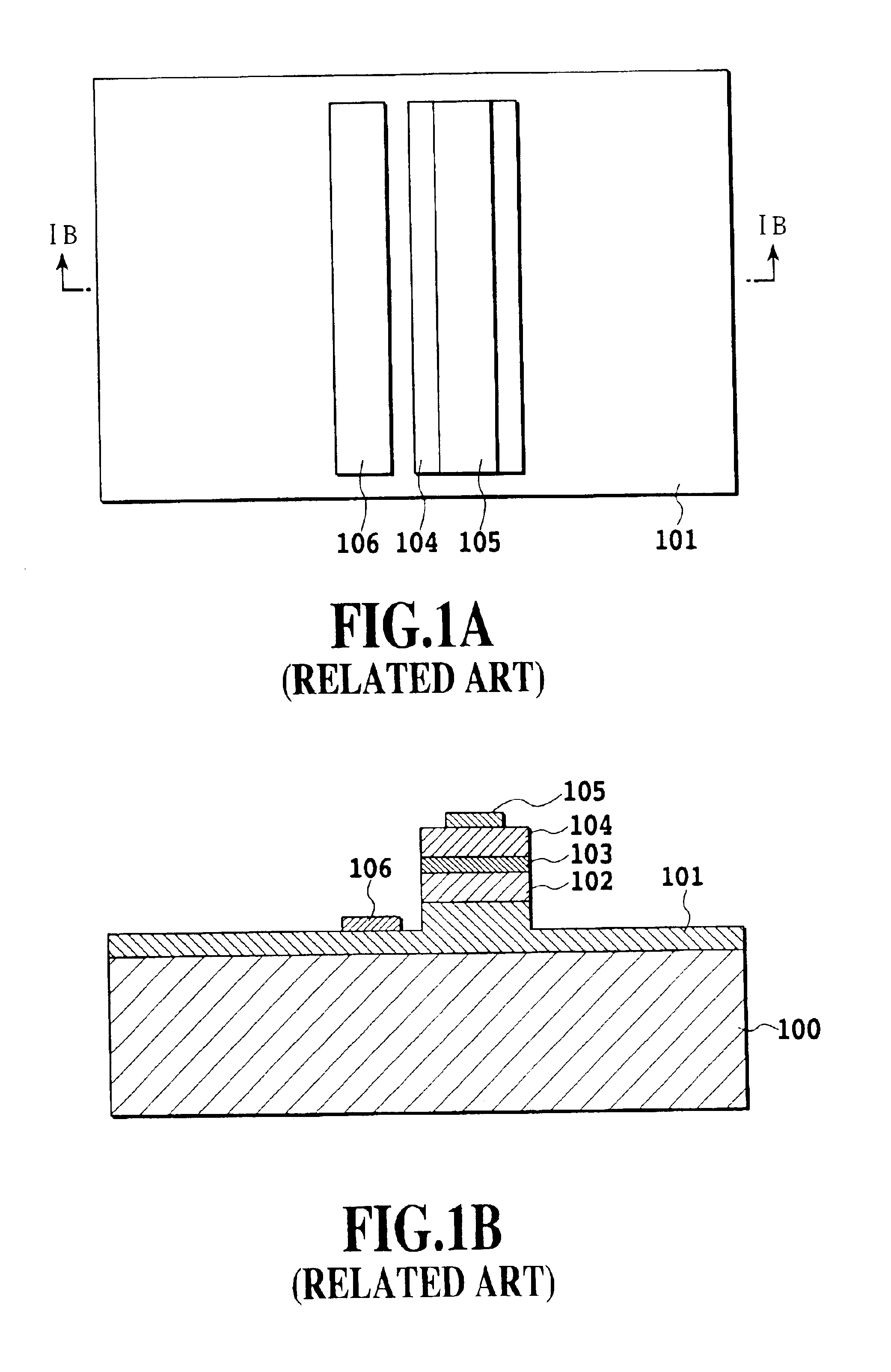
In addition, since the GaN crystal has a large band gap, there is no appropriate metallic material with a work function enabling good ohmic contact.
For these reasons, the contact resistance of the p-type GaN (p-GaN) with an electrode is order-of-magnitude greater than that of the other semiconductors, which presents a problem of preventing characteristic improvement of the light emitting devices using the nitride semiconductors.
As a result, they have a problem of increasing the laser oscillation threshold value and operation power consumption.

Method used


Image

  • Thin film deposition method of nitride semiconductor and nitride semiconductor light emitting device
  • Thin film deposition method of nitride semiconductor and nitride semiconductor light emitting device
  • Thin film deposition method of nitride semiconductor and nitride semiconductor light emitting device

Examples


example 1

[0063]FIGS. 4A, 4B, 5A and 5B are views illustrating a part of a process in the first fabrication example of the nitride semiconductor light emitting device in accordance with the present invention, when forming Mg-doped GaN thin films epitaxially by the selective-area growth using GaN crystal as the substrate: FIGS. 4A and 5A are plan views of the nitride semiconductor light emitting device in accordance with the present invention in the fabrication process; and FIGS. 4B and 5B are cross-sectional views taken along the lines IVB—IVB and VB—VB of FIGS. 4A and 5A, respectively.

[0064]FIGS. 4A and 4B illustrate a state in which a masking material 32 with stripe-like openings 31 was formed on the surface of the principal orientation plane (0001) of a GaN crystal substrate. The masking material 32 was composed of silicon dioxide (SiO2) evaporated by a sputtering system. In the present example, the thickness of the masking material 32 was 100 nm. The openings 31 were formed by photolithog...

example 2

[0073]In the present example 2, the stripe-like mask openings 31 of the foregoing example 1 were formed by a crystal growth with setting their directions parallel to the direction of the GaN crystal substrate. The remaining process and conditions were identical to those of the example 1. Thus, the side facets of the Mg-doped GaN thin films were {1-100} facets.

[0074]The Mg acquisition efficiency of the {1-100} plane of the GaN crystal was two or more orders of magnitude lower than that of the (0001) plane. Accordingly, as in the example 1, the GaN thin films formed by the selective-area growth were composed of the low resistance p-type portion formed as a result of the growth of the (0001) plane and a high resistance portion formed as a result of the growth of the {1-100} facets.

[0075]The nitride semiconductor thin films fabricated through the process in the present example 2 can also be used as a current confinement type p-type contact layer.

example 3

[0076]FIGS. 7A and 7B, and 8A and 8B are views illustrating a step of the process of fabricating a second example of the nitride semiconductor light emitting device in accordance with the present invention, which uses an n-type SiC (0001) crystal as a substrate, and includes a p-type AlGaN-based cladding layer and a p-type GaN-based cap layer: FIGS. 7A and 8A are plan views in the process of fabricating the nitride semiconductor light emitting device in accordance with the present invention; and FIGS. 7B and 8B show cross-sections along the lines VIIB—VIIB and VIIIB—VIIIB of FIGS. 7A and 8A, respectively.

[0077]FIGS. 7A and 7B are views illustrating a state of a sample after forming thin films of the nitride semiconductor functioning as the base layer of the nitride semiconductor thin films (nitride semiconductor base layer), which will be described later. The nitride semiconductor light emitting device includes a stack of an n-Al0.1Ga0.9N cladding layer 61, n-GaN optical guide layer...


PUM

PropertyMeasurementUnit
thermal energyaaaaaaaaaa
hole concentrationaaaaaaaaaa
angleaaaaaaaaaa

Abstract

A masking material 13, which includes stripe-like openings 12 parallel to the [1-100] direction of a nitride semiconductor thin film, is formed on a substrate. Nitride semiconductor thin films 11 doped with Mg are grown on the openings 12 by selective-area growth. The nitride semiconductor thin films 11 are composed of a portion 14 formed as a result of the growth in the direction perpendicular to a (0001) principal plane, and a portion 15 formed as a result of the growth of {11-2x} facets (x=0, 1, 2). The Mg concentration of the portion 15 is made lower than that of the portion 14.

Description

[0001]This application claims priority from Japanese Patent Application No. 2002-077058 filed Mar. 19, 2002, which is incorporated hereinto by reference.BACKGROUND OF THE INVENTION[0002]1. Field of the Invention[0003]The present invention relates to a nitride semiconductor light emitting device with low power consumption and / or a low laser oscillation threshold value, which reduces the contact resistance of a p-type nitride semiconductor with an electrode and the loss of injected carriers due to non-radiative surface recombination, and to a thin film deposition method of the nitride semiconductor for implementing such a device.[0004]2. Description of the Related Art[0005]A nitride semiconductor is a compound of nitrogen with at least one of III group elements B, Al, Ga and In, and includes BN, GaN, AlGaN, InGaN, AlInGaN and the like. Recently, much research and development have been done on such nitride semiconductors as light-emitting materials in short wavelength band ranging from...

Claims


Application Information

Patent Timeline
Patent Type & Authority Patents(United States)
IPC IPC(8): H01S5/323H01L33/00H01S5/00H01S5/20H01L21/20H01L21/205H01S5/343
CPCH01L21/0237H01L21/02378H01L21/02389H01L21/0242H01L21/02458H01L21/02505H01L21/0254H01L21/02579H01L21/0262H01L21/02639H01S5/32341H01L33/007H01L33/16H01S5/2077
Inventor AKASAKA, TETSUYAANDO, SEIGONISHIDA, TOSHIOKOBAYASHI, NAOKISAITOH, TADASHI
Owner NIPPON TELEGRAPH & TELEPHONE CORP
Learn More