Method of fabricating nitride semiconductor laser

a technology of nitride and semiconductor laser, which is applied in the direction of semiconductor laser, semiconductor laser structure details, semiconductor/solid-state device details, etc., can solve the problems of erroneous laser strip orientation and difficult laser strip orientation

Inactive Publication Date: 2011-05-10
SUMITOMO ELECTRIC IND LTD
View PDF19 Cites 225 Cited by
  • Summary
  • Abstract
  • Description
  • Claims
  • Application Information

AI Technical Summary

Benefits of technology

It is an object of the present invention is to provide a method of fabricating a nitride semiconductor laser on a nonpolar or semipolar wafer, and this method can facilitate to orient the laser cavity for nitride semiconductor laser on the wafer.
In the method according to the present invention, the primary surface of the hexagonal gallium nitride semiconductor wafer has an a-plane of the hexagonal gallium nitride semiconductor, and the cleavage plane of the substrate product is a c-plane of the hexagonal gallium nitride semiconductor. In this method, the first marker extends in the direction of the c-axis. The first marker permits the fabrication of a laser structure to which a c-plane cleavage can be applied.
In the method according to the present invention, the primary surface of the hexagonal gallium nitride semiconductor wafer has an m-plane of the hexagonal gallium nitride semiconductor, and the cleavage plane of the substrate product is a c-plane of the hexagonal gallium nitride semiconductor. In this method, the first marker extends in the direction of the c-axis. The first marker permits the fabrication of a laser structure to which a c-plane cleavage can be applied.
In the method according to the present invention, the substrate has a curved side surface extending in the direction of the c-axis of the hexagonal gallium nitride semiconductor, and the cutting plane intersects with the side surface of the substrate. This method enables to produce a wafer with a very large diameter. In The method according to the present invention, the cutting plane intersects the side surface and the primary surface of the substrate, but does not intersect with the back surface of the substrate. Alternatively, in The method according to the present invention, the cutting plane intersects with the side surface and the back surface of the substrate, but does not intersect with the primary surface of the substrate. According to the method, although the size of this wafer is smaller than that of the above-mentioned wafer, the substrate can be used effectively for fabricating wafers.

Problems solved by technology

In addition, it is not easy to orient the laser stripe with reference to the edge, resulting in erroneous orientation of the laser stripe.

Method used


Image

  • Method of fabricating nitride semiconductor laser
  • Method of fabricating nitride semiconductor laser
  • Method of fabricating nitride semiconductor laser

Examples


first embodiment

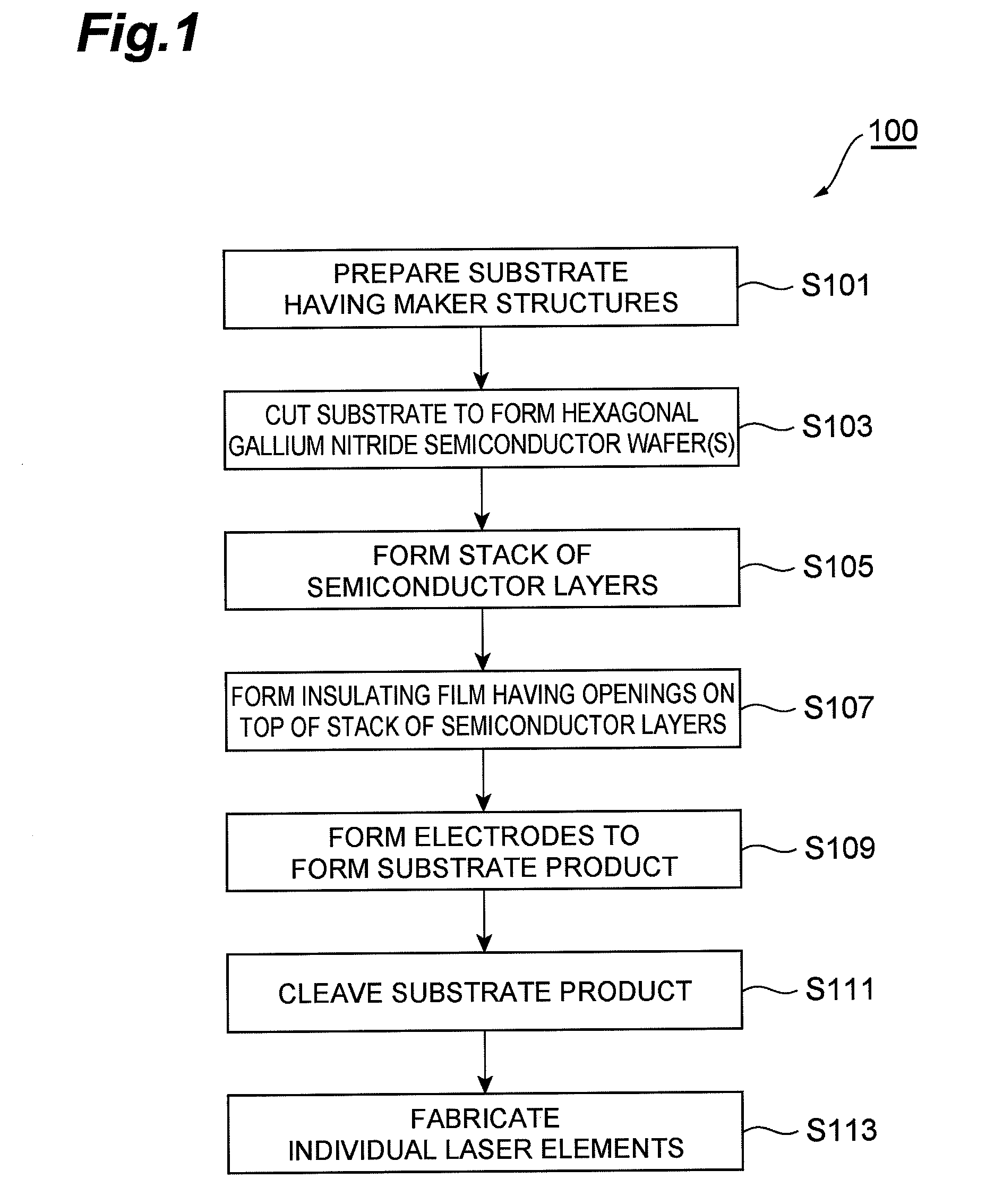
FIG. 1 is a flowchart showing primary steps of a method of fabricating a nitride semiconductor laser according to a first embodiment of the present invention. With reference to a flowchart 100 in the drawing, the method of fabricating a nitride semiconductor laser of this embodiment includes Step S101 to prepare a substrate having a plurality of marker structures, Step S103 to cut the substrate into a hexagonal gallium nitride semiconductor wafer, Step S105 to form a stack of semiconductor layers on the wafer, Step S107 to form an insulating film with openings on the stack of semiconductor layers, Step S109 to form electrodes to complete a substrate product, Step S111 to cleave the substrate product to form a laser bar, and Step S113 to divide the laser bar into separated laser devices by cutting. Each of these steps will be described in detail below.

Step S101

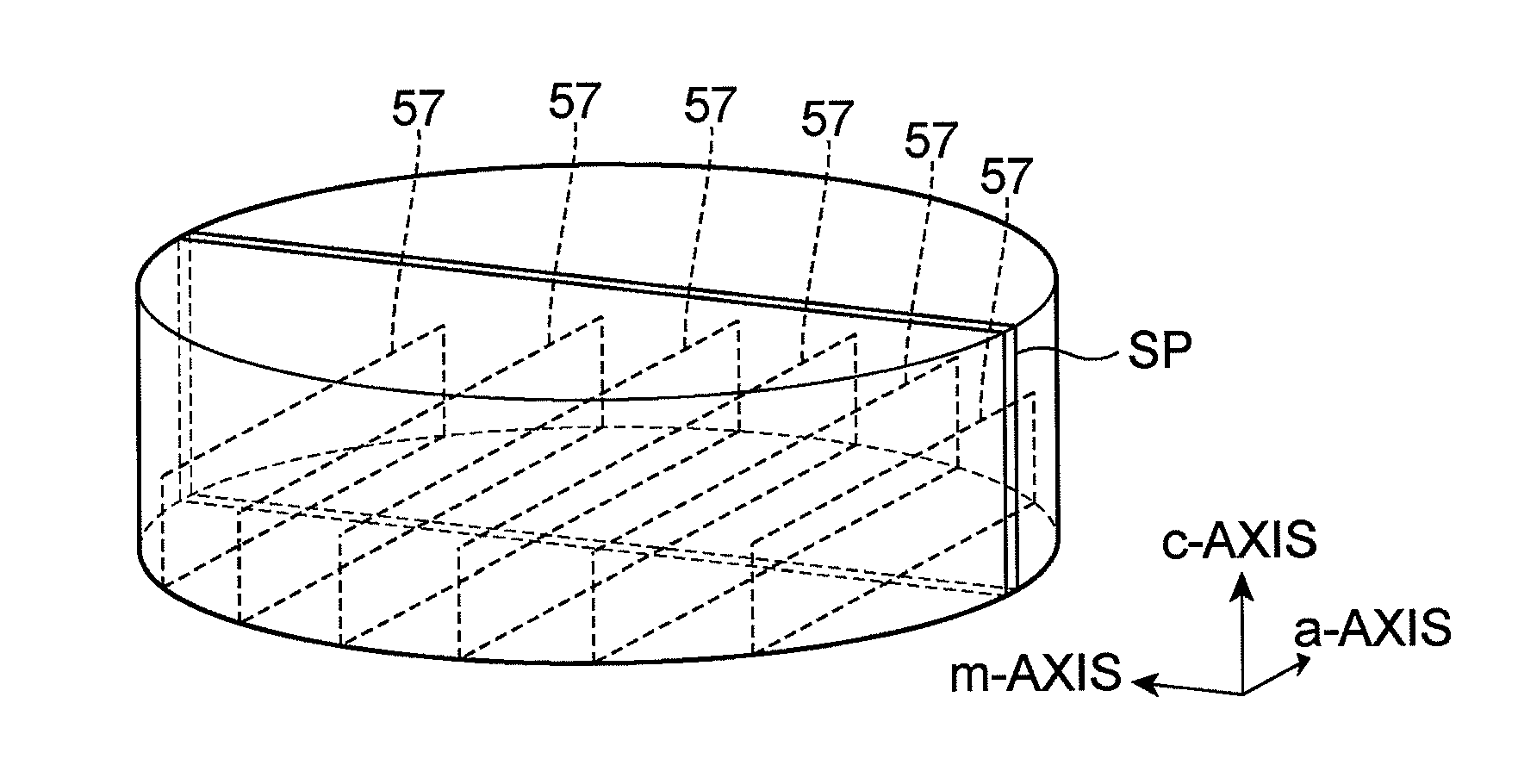
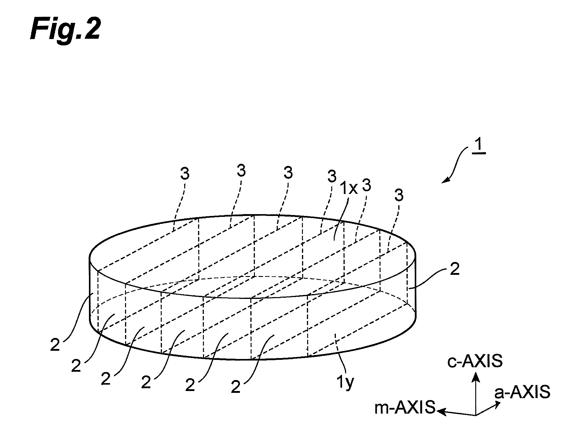
In Step S101, a substrate is prepared, and the substrate comprises a plurality of marker structures and a plurality of crysta...

second embodiment

Next, a method of fabricating a nitride semiconductor laser according to a second embodiment of the present invention will be described. In this embodiment, crystal orientation of a GaN wafer and crystalline masses having marker structures is different from that of the crystalline masses and the GaN wafer in the first embodiment.

Part (A) of FIG. 8 is a schematic view showing a substrate 1a of the present embodiment. In this embodiment, the structure of the substrate 1a is different from that of the substrate in the first embodiment in the following point: the marker structures 3a of the substrate 1a extend along a reference plane defined by the m-axis and c-axis of a GaN crystal 2a, and the reference plane is hereinafter referred to as “the m-c reference plane.”

In this embodiment, formation of the wafer is also different from that of the wafer in the first embodiment, and is described below. When the substrate 1a is cut along a cutting plane P2 intersecting with the marker structure...

third embodiment

Next, a method of fabricating a nitride semiconductor laser according to a third embodiment of the present invention will be described below. In this embodiment, crystal orientation of a GaN wafer is different from that in the first embodiment.

Part (A) of FIG. 9 is a schematic view showing a substrate 1b of this embodiment. In this embodiment, marker structures 3b are included in the substrate 1b, and each of the marker structures 3b extends along the a-c reference plane of a GaN crystal 2b.

In this embodiment, the substrate 1b is cut into a GaN wafer 5b along a cutting plane that is tilted with reference to the c-plane in the direction of the m-axis of the GaN crystal 2b by a desired off-angle α3. This cutting plane intersects with the marker structures 3b.

Part (B) of FIG. 9 is a plan view showing the GaN wafer 5b, which is formed by slicing from the substrate 1b. In this embodiment, the primary surface of the GaN wafer 5b is semipolar. FIG. 9 shows an mx-axis and a cx-axis, and t...


PUM

PropertyMeasurementUnit
angleaaaaaaaaaa
threshold currentaaaaaaaaaa
oscillation wavelengthaaaaaaaaaa

Abstract

A method of fabricating a nitride semiconductor laser comprises preparing a substrate having a plurality of marker structures and a crystalline mass made of a hexagonal gallium nitride semiconductor. The primary and back surfaces of the substrate intersect with a predetermined axis extending in the direction of a c-axis of the hexagonal gallium nitride semiconductor. Each marker structure extends along a reference plane defined by the c-axis and an m-axis of the hexagonal gallium nitride semiconductor. The method comprises cutting the substrate along a cutting plane to form a wafer of hexagonal gallium nitride semiconductor, and the cutting plane intersects with the plurality of the marker structures. The wafer has a plurality of first markers, each of which extends from the primary surface to the back surface of the wafer, and each of the first markers comprises part of each of the marker structures. The primary surface of the wafer is semipolar or nonpolar. The method comprises growing a number of gallium nitride based semiconductor layers for a semiconductor laser. The method comprises cleaving the substrate product at a cleavage plane of the hexagonal gallium nitride semiconductor, after forming a substrate product in an electrode forming step.

Description

FIELD OF THE INVENTIONThe present invention relates to a method of fabricating a nitride semiconductor laser.DESCRIPTION OF THE RELATED ARTNonpatent Document 1 (Kuniyoshi OKAMOTO et. al, “Pure Blue Laser Diodes Based on Nonpolar m-plane Gallium Nitride with InGaN Waveguiding Layers”, Japanese Journal of Applied Physics, Vol. 46, No. 35, 2007, p. L820-L822) discloses a blue laser diode. This laser diode is formed on a nonpolar m-plane gallium nitride substrate. The laser diode has an oscillation wavelength of 451.8 nm and a threshold current of 134 mA. The laser diode includes an InGaN quantum well structure, a p-type GaN or InGaN optical waveguide layer, an n-type GaN or InGaN optical waveguide layer, and an Al-containing cladding layer.SUMMARY OF THE INVENTIONA light emitting device such as a semiconductor laser can be formed on a nonpolar GaN substrate or a semipolar GaN substrate. The nonpolar GaN substrate and the semipolar GaN substrate for the light-emitting device can be fabr...

Claims


Application Information

Patent Timeline
Patent Type & Authority Patents(United States)
IPC IPC(8): H01L21/00
CPCB82Y20/00H01S5/34333H01S5/0202H01S2304/12H01S5/3202H01S5/2009H01S5/32025H01S5/320275H01S5/02H01S5/026
Inventor KYONO, TAKASHIAKITA, KATSUSHIYOSHIZUMI, YUSUKE
Owner SUMITOMO ELECTRIC IND LTD
Why Eureka
Try Eureka