Semiconductor device and method for manufacturing semiconductor device

a semiconductor and semiconductor technology, applied in the direction of semiconductor devices, electrical equipment, transistors, etc., can solve the problems of unstable electric characteristics of transistors, and achieve the effect of stable electric characteristics and highly reliable semiconductor devices

Active Publication Date: 2012-05-31
SEMICON ENERGY LAB CO LTD
View PDF3 Cites 161 Cited by
  • Summary
  • Abstract
  • Description
  • Claims
  • Application Information

AI Technical Summary

Benefits of technology

[0007]Electric characteristics of a transistor are easily affected by the condition of an interface between an oxide semiconductor film serving as an active layer and a gate insulating film in contact with the oxide semiconductor film. During or after manufacture of the transistor, if the interface where the gate insulating film is in contact with the oxide semiconductor film, that is, the gate-electrode-side interface of the oxide semiconductor film is in an amorphous state, the structural condition is easily changed by an influence of temperature or the like in the manufacturing process and electric characteristics of the transistor are likely to be unstable.

Problems solved by technology

During or after manufacture of the transistor, if the interface where the gate insulating film is in contact with the oxide semiconductor film, that is, the gate-electrode-side interface of the oxide semiconductor film is in an amorphous state, the structural condition is easily changed by an influence of temperature or the like in the manufacturing process and electric characteristics of the transistor are likely to be unstable.

Method used


Image

  • Semiconductor device and method for manufacturing semiconductor device
  • Semiconductor device and method for manufacturing semiconductor device
  • Semiconductor device and method for manufacturing semiconductor device

Examples


embodiment 1

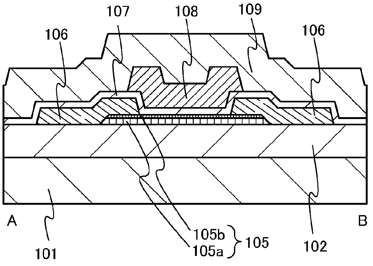
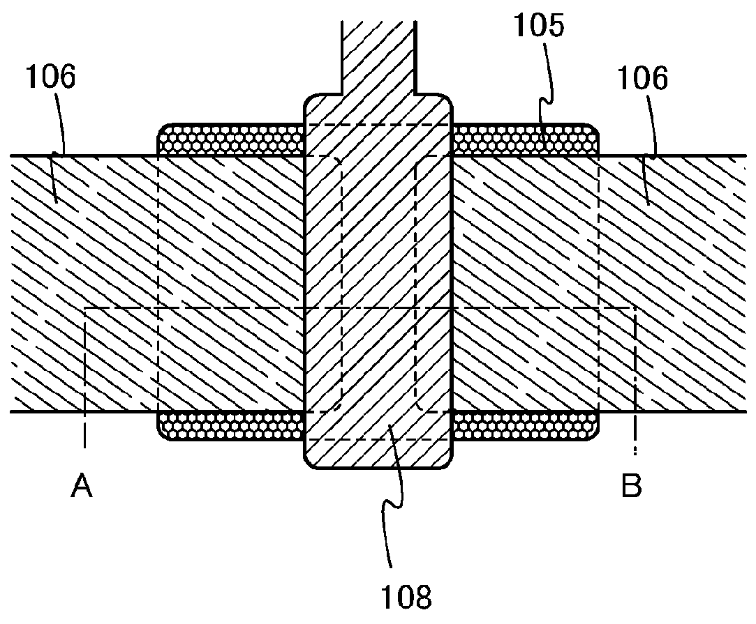
[0051]In this embodiment, a transistor in which an oxide semiconductor film over an insulating surface is used for a channel and a manufacturing method thereof will be described with reference to FIGS. 1A and 1B and FIGS. 2A to 2C. FIG. 1B is a cross-sectional view illustrating a structure of a transistor which is one embodiment of a structure of a semiconductor device, and corresponds to a cross-sectional view along dashed-dotted line A-B in FIG. 1A which is a top view. Note that in FIG. 1A, a substrate 101, an oxide insulating film 102, a gate insulating film 107, and an insulating film 109 are not illustrated. FIGS. 2A to 2C are cross-sectional views illustrating a manufacturing process of the transistor illustrated in FIG. 1B.

[0052]The transistor illustrated in FIG. 1B includes the oxide insulating film 102 formed over the substrate 101; an oxide semiconductor stack 105 formed over the oxide insulating film 102; a pair of electrodes 106 which is formed over the oxide semiconduct...

embodiment 2

[0145]In this embodiment, a structure of a transistor which is different from that in Embodiment 1 and a manufacturing method thereof will be described with reference to FIGS. 7A and 7B and FIGS. 8A to 8C. This embodiment is different from Embodiment 1 in that a pair of electrodes is provided between an oxide insulating film and an oxide semiconductor stack. Note that FIG. 7B corresponds to a cross-sectional view along dashed-dotted line C-D in FIG. 7A which is a top view. In FIG. 7A, the substrate 101, the oxide insulating film 102, a gate insulating film 117, and an insulating film 119 are not illustrated. FIGS. 8A to 8C are cross-sectional views illustrating a manufacturing process of the transistor illustrated in FIG. 7B.

[0146]The transistor illustrated in FIG. 7B includes the oxide insulating film 102 formed over the substrate 101; a pair of electrodes 116 which is formed over the oxide insulating film 102 and functions as a source electrode and a drain electrode; an oxide semi...

embodiment 3

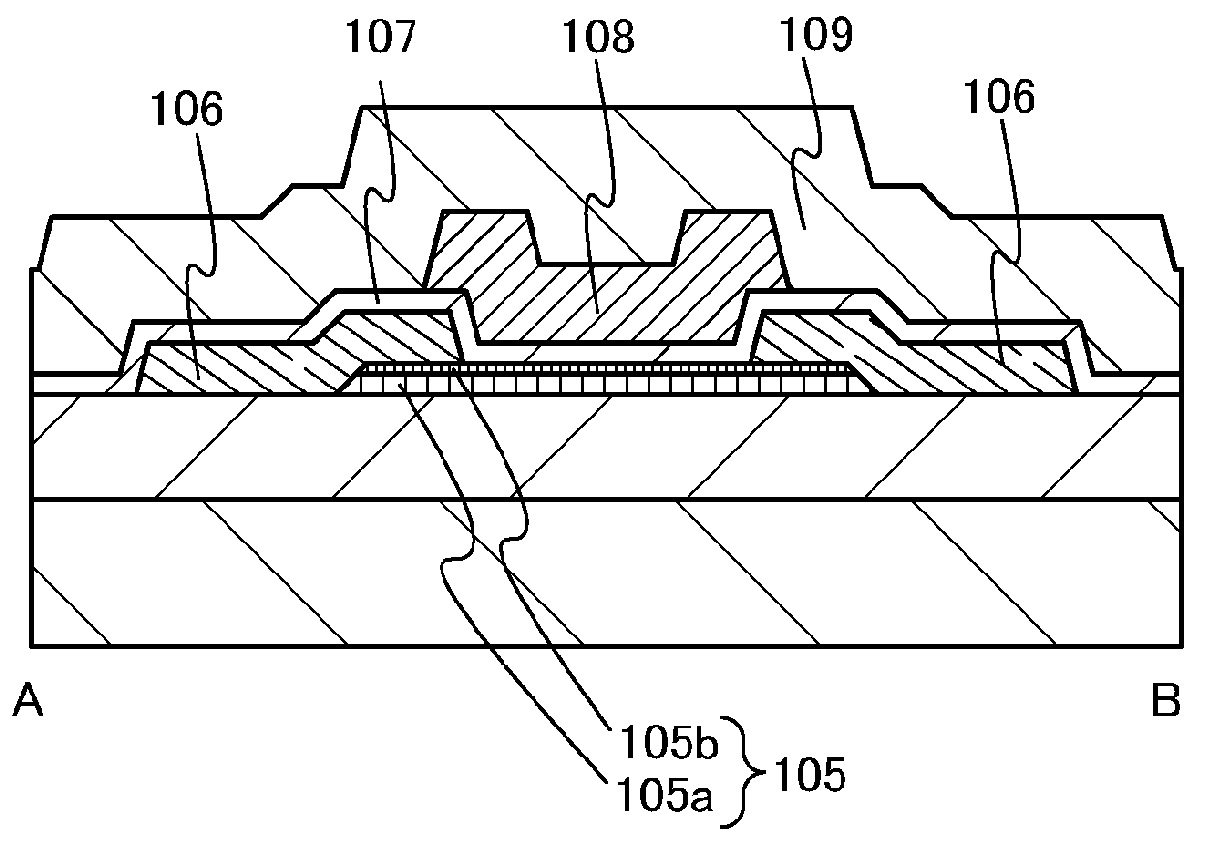
[0168]In this embodiment, a transistor in which an oxide semiconductor film is used for a channel and a manufacturing method thereof will be described with reference to FIGS. 9A and 9B and FIGS. 10A to 10E. FIG. 9B is a cross-sectional view illustrating a structure of a transistor which is one embodiment of a structure of a semiconductor device, and corresponds to a cross-sectional view along dashed-dotted line A-B in FIG. 9A which is a top view. Note that in FIG. 9A, the substrate 101, the oxide insulating film 102, the gate insulating film 107, and the insulating film 109 are not illustrated. FIGS. 10A to 10E are cross-sectional views illustrating a manufacturing process of the transistor illustrated in FIG. 9B.

[0169]The transistor illustrated in FIG. 9B includes the oxide insulating film 102 formed over the substrate 101; the oxide semiconductor stack 105 formed over the oxide insulating film 102; the pair of electrodes 106 which is formed over the oxide semiconductor stack 105 a...


PUM


Abstract

A highly reliable semiconductor device is manufactured by giving stable electric characteristics to a transistor in which an oxide semiconductor film is used for a channel. An oxide semiconductor film which can have a first crystal structure by heat treatment and an oxide semiconductor film which can have a second crystal structure by heat treatment are formed so as to be stacked, and then heat treatment is performed; accordingly, crystal growth occurs with the use of an oxide semiconductor film having the second crystal structure as a seed, so that an oxide semiconductor film having the first crystal structure is formed. An oxide semiconductor film formed in this manner is used for an active layer of the transistor.

Description

TECHNICAL FIELD[0001]The present invention relates to a semiconductor device which includes a circuit including a semiconductor element such as a transistor, and a method for manufacturing the semiconductor device. For example, the present invention relates to a power device which is mounted on a power supply circuit; a semiconductor integrated circuit including a memory, a thyristor, a converter, an image sensor, or the like; and an electronic device on which an electro-optical device typified by a liquid crystal display panel, a light-emitting display device including a light-emitting element, or the like is mounted as a component.[0002]In this specification, a semiconductor device means all types of devices which can function by utilizing semiconductor characteristics, and an electro-optical device, a light-emitting display device, a semiconductor circuit, and an electronic device are all semiconductor devices.BACKGROUND ART[0003]A transistor formed over a glass substrate or the ...

Claims


Application Information

Patent Timeline
Patent Type & Authority Applications(United States)
IPC IPC(8): H01L29/786H01L21/34
CPCH01L21/0242H01L29/24H01L21/02472H01L21/02483H01L21/02502H01L21/02513H01L21/02554H01L21/02565H01L21/0259H01L29/7869H01L29/78693H01L29/66969H01L21/02631H01L21/02667H01L29/04H01L21/02422H01L27/1225H01L29/66742H01L29/78696H01L29/36H01L29/06
Inventor YAMAZAKI, SHUNPEITAKAHASHI, MASAHIROMARUYAMA, TETSUNORI
Owner SEMICON ENERGY LAB CO LTD
Why Eureka
Try Eureka