Photosensing thin film transistor

a thin film transistor and photosensitive technology, applied in the field of photosensitive thin film transistors, can solve the problems of slow response time and drain current decay within a time frame ranging from seconds to tens of seconds, and achieve the effect of improving photosensitivity and fast response tim

a thin film transistor and photosensitive technology, applied in the field of photosensitive thin film transistors, can solve the problems of slow response time and drain current decay within a time frame ranging from seconds to tens of seconds, and achieve the effect of improving photosensitivity and fast response tim

US20070257256A1Inactive Publication Date: 2007-11-08SEIKO EPSON CORP

Image

  • Photosensing thin film transistor
  • Photosensing thin film transistor
  • Photosensing thin film transistor

Examples


Embodiment Construction

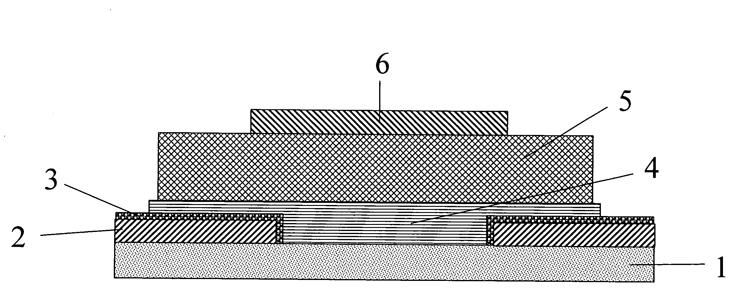
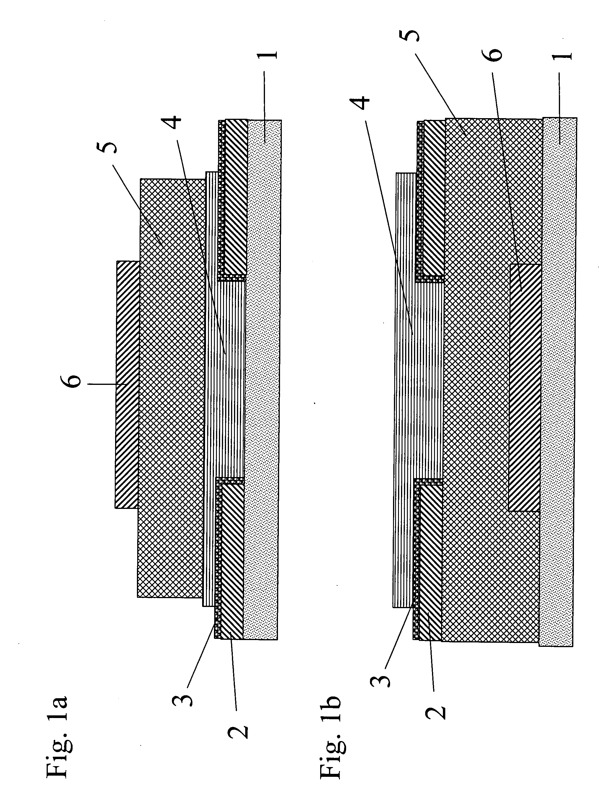
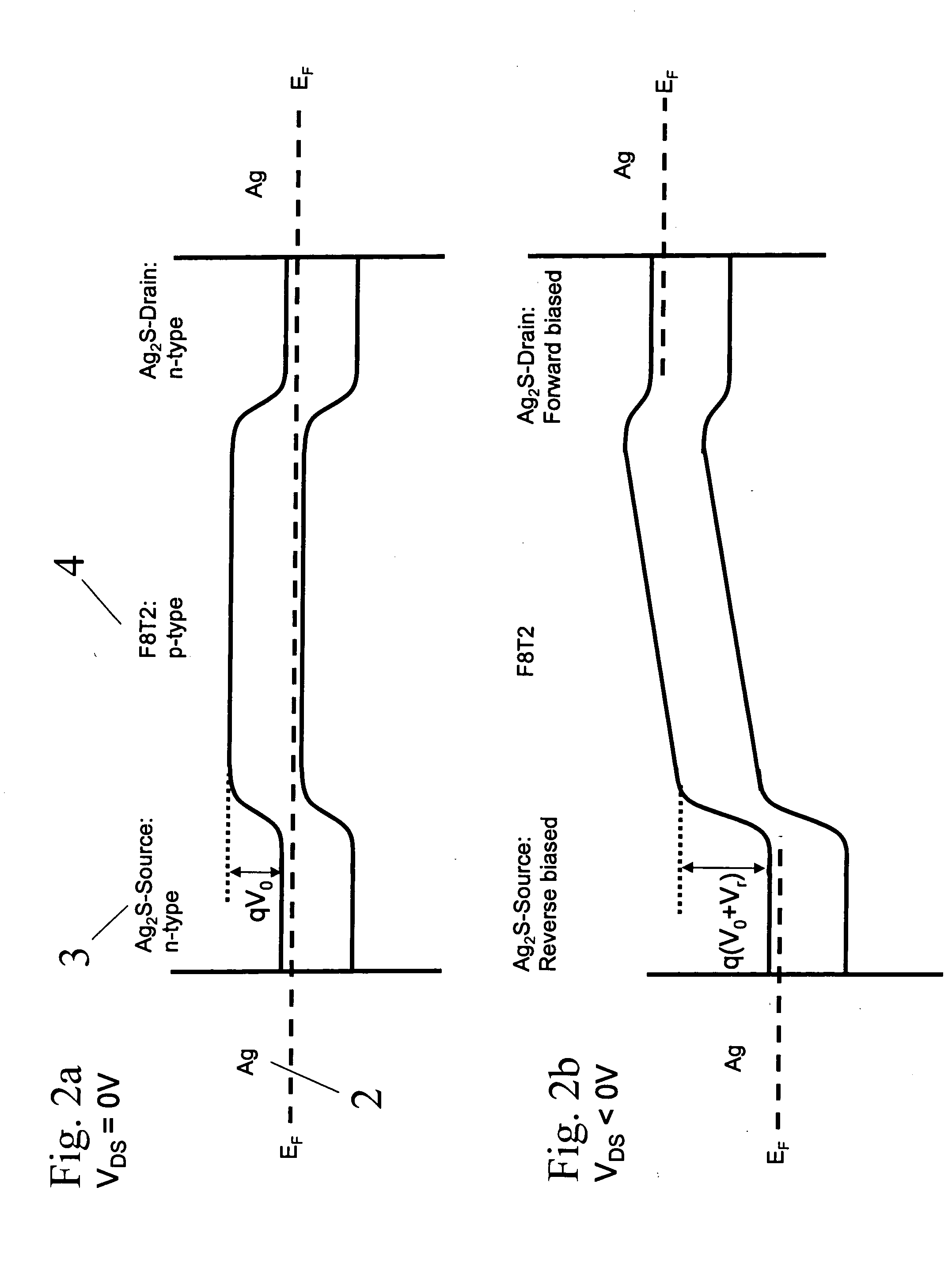
[0046]One embodiment of the present invention is a photosensing hybrid organic / inorganic thin film transistor (PHOITFT) comprising an insulating substrate with a substrate surface, a semiconductor organic layer, an electrically conducting source electrode that is covered with a thin photoconducting semiconductor coating, said semiconductor coating being in electrical contact with the organic semiconductor layer, an electrically conducting drain electrode that is covered with a thin photoconducting semiconductor coating, said semiconductor coating being in electrical contact with the organic semiconductor layer, an insulating layer, and an optically transparent and electrically conducting gate electrode positioned adjacent to the insulating layer.

[0047]The thin photoconducting semiconductor coatings on the source contact and on the drain contact are of the opposite conductivity type as compared to the material of the organic semiconductor layer, i.e. n-type in case of a p-type organi...


PUM

PropertyMeasurementUnit
thicknessaaaaaaaaaa
light absorption coefficientaaaaaaaaaa
gate voltagesaaaaaaaaaa

Abstract

A thin film transistor (TFT) photosensitive to illumination with light, which may enhance the transistor's characteristics and the controlling parameters of the transistor state. The transistor comprises an insulating substrate; a source electrode; a drain electrode; a semiconductor layer of a first semiconductor material, which forms a channel of the transistor; a gate electrode; and an insulating layer between the gate electrode and the semiconductor layer. A second semiconductor material is disposed between and in electrical connection with the semiconductor layer and at least one of the source electrode and the drain electrode. The second semiconductor material is photoconductive.

Description

FIELD OF THE INVENTION[0001]The present invention relates to photosensitive thin film transistors (TFTs) and methods for producing them.BACKGROUND OF THE INVENTION[0002]Organic thin film transistors (OTFTs) have gained considerable interest due to their potential application in low cost integrated circuits and large area flat panel displays. Although the highest device performance in terms of field effect mobility is observed in devices incorporating films of evaporated small molecules, research into polymer semiconductors remains at a high level of activity as they are intrinsically compatible with printing technologies in ambient conditions.[0003]Possible applications of OTFTs include printed poly(3-hexylthiophene) (P3HT)-based printed integrated circuits, as disclosed by A. Knobloch, A. Manuelli, A. Bernds, W. Clemens, “Fully printed integrated circuits from solution processable polymers”, J. Appl. Phys., vol. 96, (2004); pentacene-based OTFTs integrated with organic light-emitti...

Claims


Application Information

Patent Timeline
08 Nov 2007
Publication
US20070257256A1
IPC
H01L29/08
CPC
B82Y10/00; H01L51/0036; H01L51/0037; H01L51/0039; H01L51/0043; H01L51/0047; Y02E10/549; H01L51/0541
Inventors
KUGLER, THOMAS