Unlock instant, AI-driven research and patent intelligence for your innovation.

Semiconductor device having plural memory chip

a memory chip and semiconductor technology, applied in the field of semiconductor devices, can solve the problems of increasing the number of read/write buses required, difficult to stack a large number of memory chips, and increasing the wiring length significantly

Active Publication Date: 2012-05-31
LONGITUDE LICENSING LTD
View PDF15 Cites 39 Cited by
  • Summary
  • Abstract
  • Description
  • Claims
  • Application Information

AI Technical Summary

Problems solved by technology

This makes it difficult to stack a large number of memory chips.
Distributing the read data to different through silicon vias chip by chip therefore has the problem of not only increasing the number of read / write buses required but also increasing the wiring lengths significantly.

Method used


Image

  • Semiconductor device having plural memory chip
  • Semiconductor device having plural memory chip
  • Semiconductor device having plural memory chip

Examples


Embodiment Construction

[0027]Preferred embodiments of the present invention will be explained below in detail with reference to the accompanying drawings.

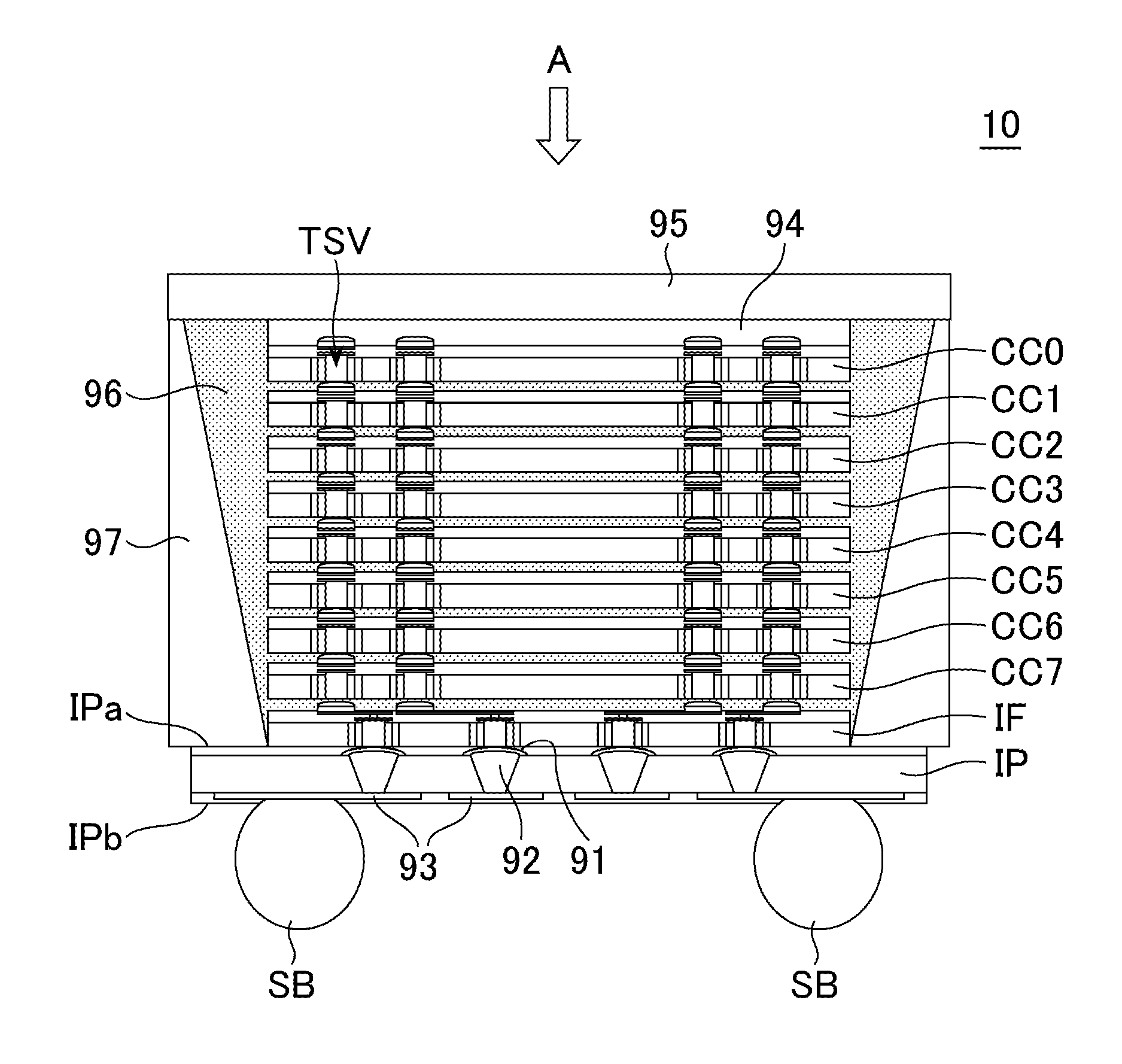
[0028]Referring now to FIG. 1, the semiconductor device 10 according to this embodiment has the structure where eight core chips (memory chips) CC0 to CC7 that have the same function and structure and are manufactured using the same manufacture mask, an interface chip IF that is manufactured using a manufacture mask different from that of the core chips and an interposer IP are laminated. The core chips CC0 to CC7 and the interface chip IF are semiconductor chips using a silicon substrate and are electrically connected to adjacent chips in a vertical direction through plural Through Silicon Vias (TSV) penetrating the silicon substrate. The through silicon vias may be referred to as penetration electrodes. Meanwhile, the interposer IP is a circuit board that is made of a resin, and plural external terminals (solder balls) SB are formed in a back surface I...


PUM


Abstract

A semiconductor device includes a stacked plurality of memory chips. The memory chips each include a plurality of memory banks, a plurality of read / write buses that are assigned to the respective memory banks, and a plurality of penetration electrodes that are assigned to the respective read / write buses and arranged through the memory chip. Penetration electrodes arranged in the same positions as seen in a stacking direction are connected in common between the chips. In response to an access request, the memory chips activate the memory banks that are arranged in respective different positions as seen in the stacking direction, whereby data is simultaneously input / output via the penetration electrodes that lie in different planar positions.

Description

BACKGROUND OF THE INVENTION[0001]1. Field of the Invention[0002]The present invention relates to a semiconductor device, and more particularly to a semiconductor device includes a stacked plurality of semiconductor memory chips.[0003]2. Description of Related Art[0004]Storage capacities required to semiconductor memories such as a dynamic random access memory (DRAM) have been increasing year by year. To satisfy such a request, a semiconductor memory device called multi-chip package has recently been proposed in which a plurality of memory chips are stacked on each other. In a multi-chip package, wirings for connecting a memory chip with the package substrate need to be provided each memory chip. This makes it difficult to stack a large number of memory chips.[0005]In view of this, there has recently been proposed a type of semiconductor device in which a plurality of memory chips having through silicon vias are stacked (see Japanese Patent Application Laid-Open Nos. 2002-305283 and ...

Claims


Application Information

Patent Timeline
IPC IPC(8): G11C5/02
CPCH01L23/481H01L25/0657H01L23/50H01L2224/16145G11C5/04G06F12/0292G06F2212/1041G11C11/408H01L2225/06544
Inventor IDE, AKIRA
Owner LONGITUDE LICENSING LTD