Semiconductor Structures and Method for Fabricating the Same

Inactive Publication Date: 2012-05-31
HIMAX TECH LTD
View PDF4 Cites 4 Cited by
  • Summary
  • Abstract
  • Description
  • Claims
  • Application Information

AI Technical Summary

Benefits of technology

[0008]The invention provides a plurality of uniform spacers with the same thickness between substrates to support the substrate during a bonding process such that the gap between the substrates is controlled, effectively improving bonding uniformity. Specifically, due to the disposition of the spacer, an adhesive material is restricted within the two adjacent

Problems solved by technology

However, the patterned photo-sensitive material with various thicknesses formed by photolithography is non-uniform, thus deteriorating bonding uniformity.
Also, the pho

Method used


Image

  • Semiconductor Structures and Method for Fabricating the Same
  • Semiconductor Structures and Method for Fabricating the Same
  • Semiconductor Structures and Method for Fabricating the Same

Examples


Embodiment Construction

[0015]The following description is of the best-contemplated mode of carrying out the invention. This description is made for the purpose of illustrating the general principles of the invention and should not be taken in a limiting sense. The scope of the invention is best determined by reference to the appended claims.

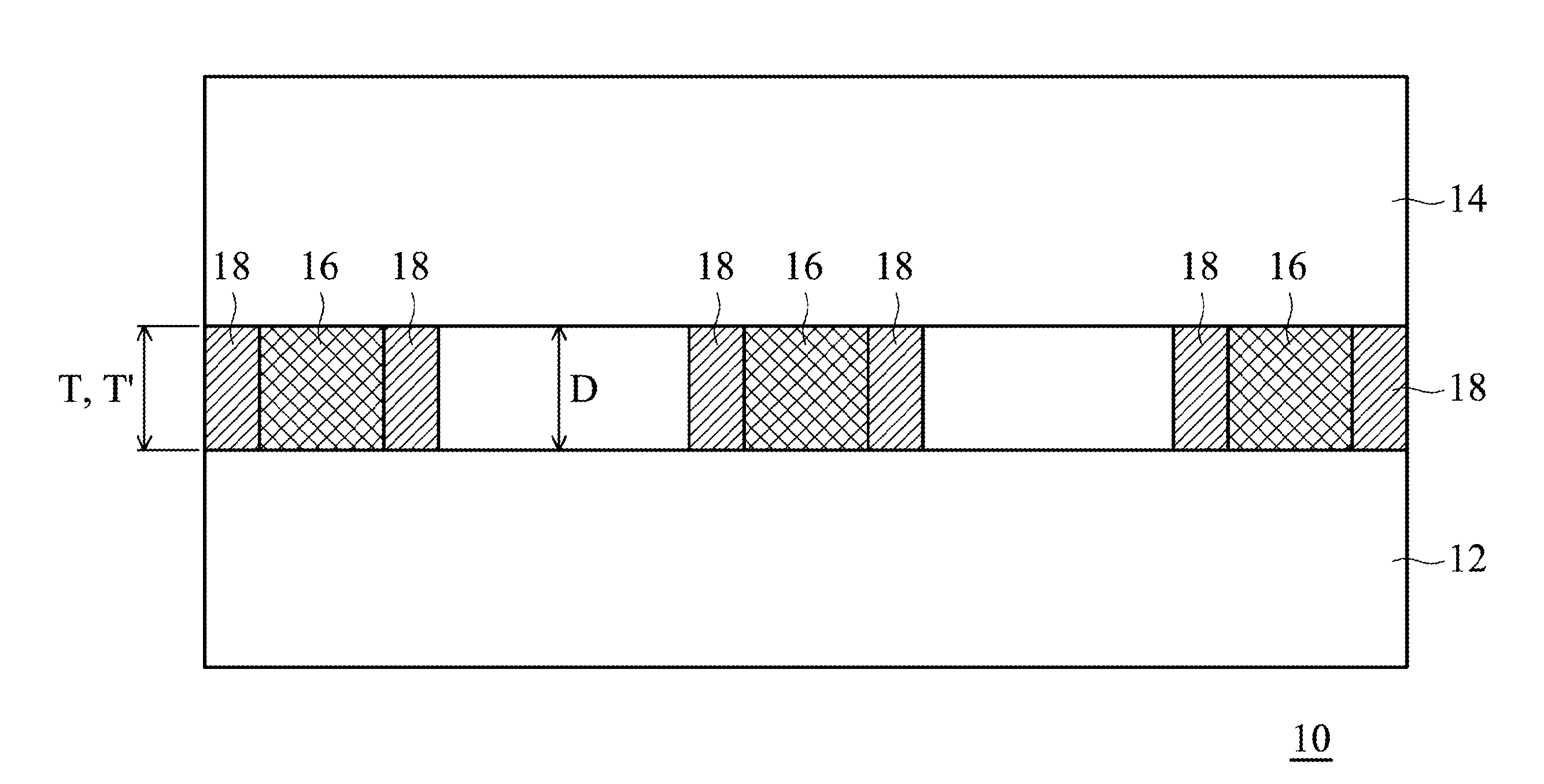
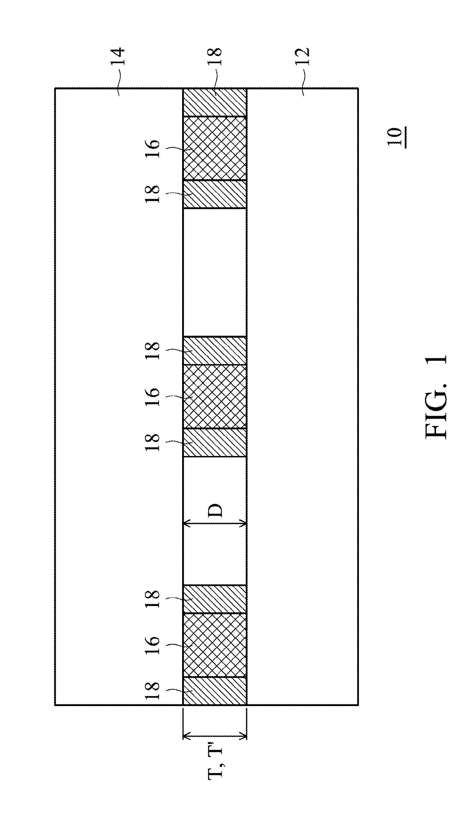
[0016]In one embodiment, a semiconductor structure is provided, as shown in FIG. 1. A semiconductor structure 10 comprises a first substrate 12, a second substrate 14, a plurality of spacers 16 and an adhesive material 18. The second substrate 14 is opposite to the first substrate 12. The spacers 16 are disposed between the first substrate 12 and the second substrate 14. The adhesive material 18 is bonded with the first substrate 12 and the second substrate 14 within the two adjacent spacers 16.

[0017]The first substrate 12 may comprise a wafer. The second substrate 14 may comprise glass. The spacer 16 may comprise plastics. The adhesive material 18 may comprise non-pho...


PUM

PropertyMeasurementUnit
Thicknessaaaaaaaaaa
Structureaaaaaaaaaa
Widthaaaaaaaaaa

Abstract

A semiconductor structure is provided. The semiconductor structure includes a first substrate, a second substrate opposite to the first substrate, a plurality of spacers disposed between the first substrate and the second substrate, and an adhesive material bonded with the first substrate and the second substrate within the two adjacent spacers. The invention also provides a method for fabricating the semiconductor structure.

Description

BACKGROUND OF THE INVENTION[0001]1. Field of the Invention[0002]The invention relates to a semiconductor structure, and more particularly to a semiconductor structure with a spacer disposed between substrates and a fabrication method thereof.[0003]2. Description of the Related Art[0004]A conventional method of bonding is disclosed as follows. First, a photo-sensitive material is applied on a substrate. After photolithography, a patterned photo-sensitive material is formed on the substrate. Another substrate is then bonded to the substrate through the photo-sensitive material. However, the patterned photo-sensitive material with various thicknesses formed by photolithography is non-uniform, thus deteriorating bonding uniformity. Also, the photo-sensitive material is easily deformed (outflow) during the bonding process. Additionally, the bonding force of the photo-sensitive material to the substrates is weak.[0005]Thus, development of a novel bonding method which is able to improve th...

Claims


Application Information

Patent Timeline
IPC IPC(8): B32B3/22B32B37/02
CPCB32B7/14Y10T428/24744B32B37/12B32B2313/00B32B2457/14H01L24/94B32B17/06Y10T428/24562Y10T156/10Y10T428/24826H01L2224/8134H01L2224/94H01L2224/81201H01L2224/81191H01L2224/81139H01L2224/16227H01L2224/1601H01L2224/1319H01L2224/13099H01L2224/13082H01L24/13H01L24/16H01L24/81H01L2224/10135H01L2224/11436H01L2224/1163H01L2224/81H01L2924/00014H01L2924/00012H01L2224/16225H01L24/11
Inventor CHANG, TSUNG-CHIEHKO, CHING-HUNGLIU, MU-JIA
Owner HIMAX TECH LTD
Why Eureka
Try Eureka