Semiconductor device and method of manufacturing the same

a technology of semiconductor devices and heat dissipation characteristics, which is applied in the direction of semiconductor devices, semiconductor/solid-state device details, electrical devices, etc., can solve the problems of high cost of composite materials, degeneration of heat dissipation characteristics of heat dissipating elements, and limited reliability, so as to achieve satisfactory productivity, reduce cost, and respond to temperature changes. , the effect of low cos

Inactive Publication Date: 2012-06-07
MITSUBISHI ELECTRIC CORP
View PDF5 Cites 11 Cited by
  • Summary
  • Abstract
  • Description
  • Claims
  • Application Information

AI Technical Summary

Benefits of technology

[0010]The present invention has been made in view of the aforementioned problems. It is an object of the present invention to provide a semiconductor device and a method of manufacturing the same capable of reliably responding to temperature change while achieving satisfactory productivity at low cost.

Problems solved by technology

The semiconductor device disclosed in patent literature 1 allows the insulating layer and the cooler constituting the insulating layer to be secured to each other only with a limited level of reliability.
Thus, a crack due to thermal stress may be generated, or thermal resistance may be increased as a result of development of the crack, leading to degeneration of the heat dissipation characteristics of a heat dissipating element.
However, such a composite material is very costly.
However, it is difficult to press a large number of stacked coolers each having a surface with irregularities to which the insulating sheet is stuck, resulting in poor productivity during hot pressing.

Method used


Image

  • Semiconductor device and method of manufacturing the same
  • Semiconductor device and method of manufacturing the same
  • Semiconductor device and method of manufacturing the same

Examples


first preferred embodiment

Structure

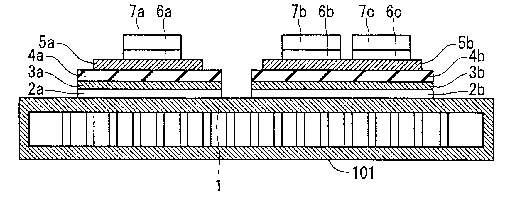
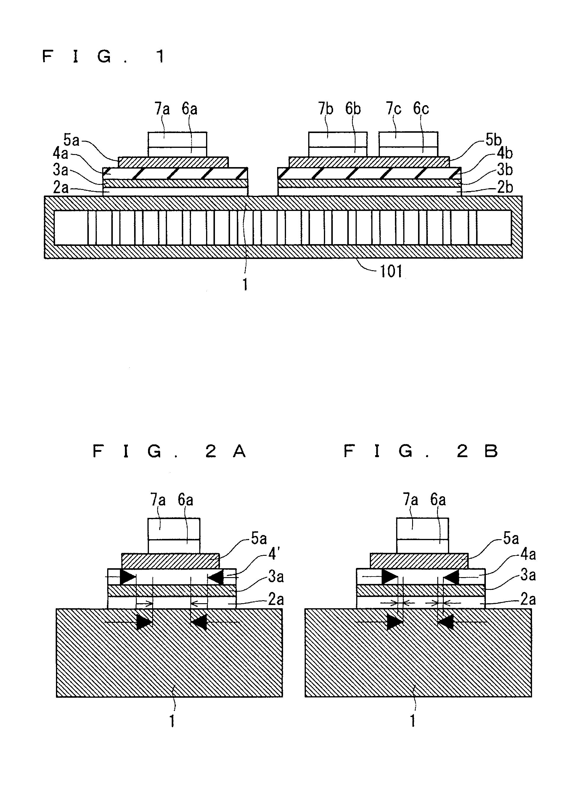
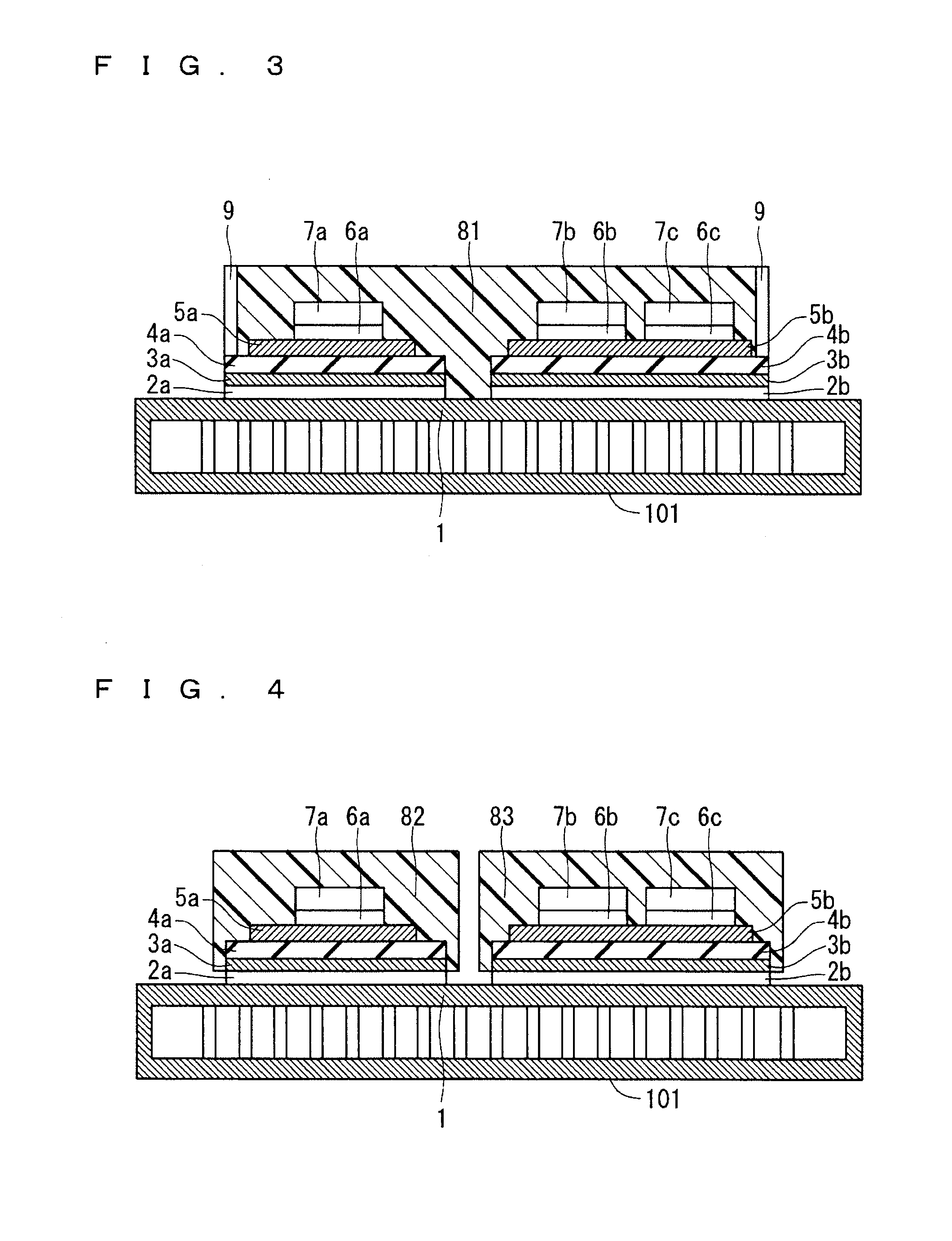
[0020]FIG. 1 is a sectional view of the structure of a semiconductor device of a first preferred embodiment. The semiconductor device of the first preferred embodiment includes a cooler 101 with a metal base 1 constituting one main surface of the cooler 101 and functioning as a top plate, and a joined layer 3a secured to the metal base 1 through a joining layer 2a. The joined layer 3a and an insulating layer 4a formed on the joined layer 3a are formed integrally with each other for example by film coating, pressing, or adhesive bonding. A metal layer 5a is formed on the insulating layer 4a. A semiconductor element 7a is formed over the metal layer 5a through a joining layer 6a.

[0021]That is, the joining layer 2a, the joined layer 3a, the insulating layer 4a, the metal layer 5a, the joining layer 6a, and the semiconductor element 7a are provided in this order over the metal base 1 into a stacked structure, and a plurality of stacked structures is formed on the metal base 1....


PUM

PropertyMeasurementUnit
band gapaaaaaaaaaa
heat conductivityaaaaaaaaaa
stressaaaaaaaaaa

Abstract

A semiconductor device includes a cooler having a main surface constructed of a metal base, joined layers fixed on the metal base through joining layers, insulating layers fixed on the joined layers and which contain an organic resin as a base material, metal layers provided on the insulating layers, and semiconductor elements provided on the metal layers. A stacked structure with the joined layers, the insulating layers, and the metal layers is divided into parts containing one or the plurality of semiconductor elements, and is fixed through the joining layers on the metal base.

Description

BACKGROUND OF THE INVENTION[0001]1. Field of the Invention[0002]The present invention relates to a semiconductor device with means for cooling a semiconductor element.[0003]2. Description of the Background Art[0004]The conventional structure of a semiconductor device is such that metal plates are stuck on upper and lower sides of an insulating plate made of ceramic, one of the metal plates is secured by soldering on a metal base, and an element is placed on the other one of the metal plates (see patent literature 1: Japanese Patent Application Laid-Open No. 2003-204021). Further, the metal base is secured on a surface of a cooler for example by the following way mainly employed: grease is interposed between the metal base and the cooler, and then the metal base and the cooler are fastened to each other with a screw.[0005]In order to enhance heat dissipation characteristics, an insulating layer may be stuck directly on a surface of a cooler to eliminate the need of grease of poor hea...

Claims


Application Information

Patent Timeline
Patent Type & Authority Applications(United States)
IPC IPC(8): H01L23/34H01L21/50
CPCH01L23/3735H01L23/4334H01L2224/32225H01L25/072H01L23/473
Inventor KIKUCHI, MASAOUSUI, OSAMU
Owner MITSUBISHI ELECTRIC CORP
Why Eureka
Try Eureka