

Semiconductor device
a technology of semiconductor devices and insulating films, applied in semiconductor devices, semiconductor/solid-state device details, electrical devices, etc., can solve the problems of affecting the effect of interwiring capacitance, so as to suppress the increase of interwiring capacitance, the effect of sufficient margin and efficient dummy pattern formation
- Summary
- Abstract
- Description
- Claims
- Application Information
AI Technical Summary
Benefits of technology
Problems solved by technology
Method used
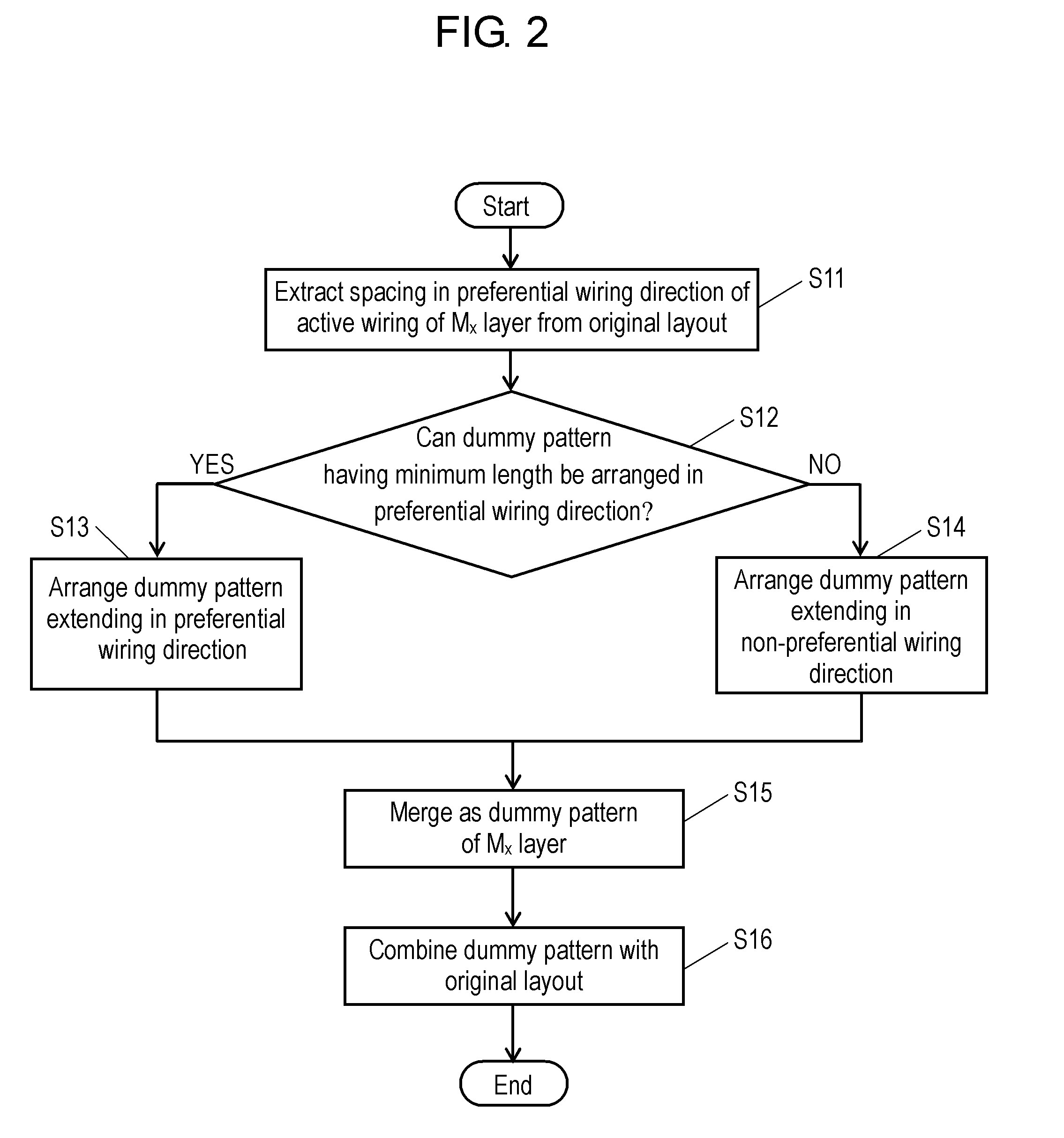
Image

Examples
first exemplary embodiment
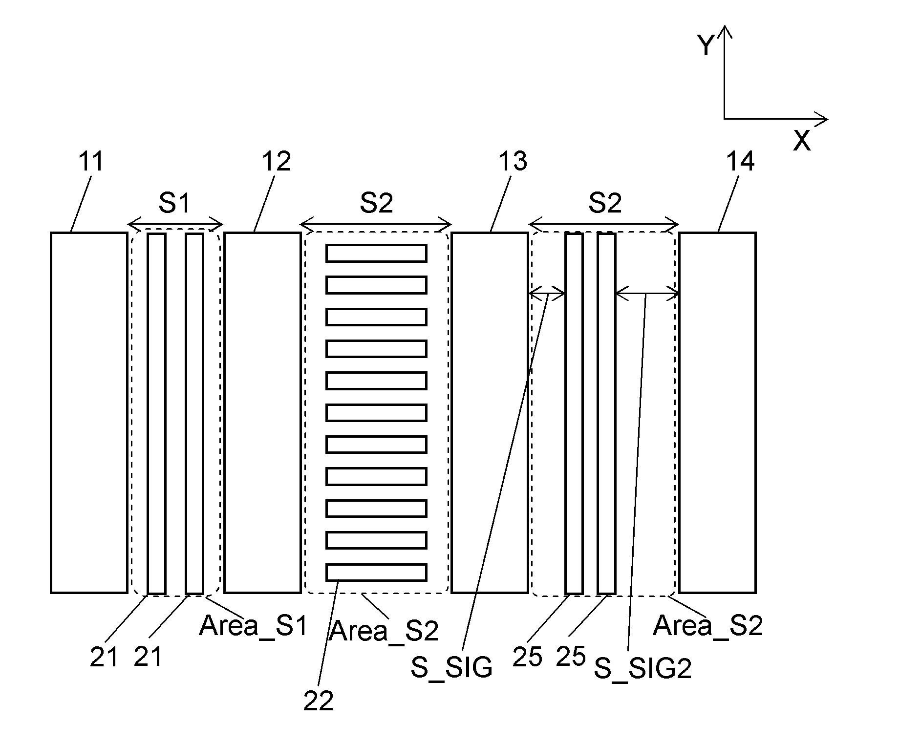
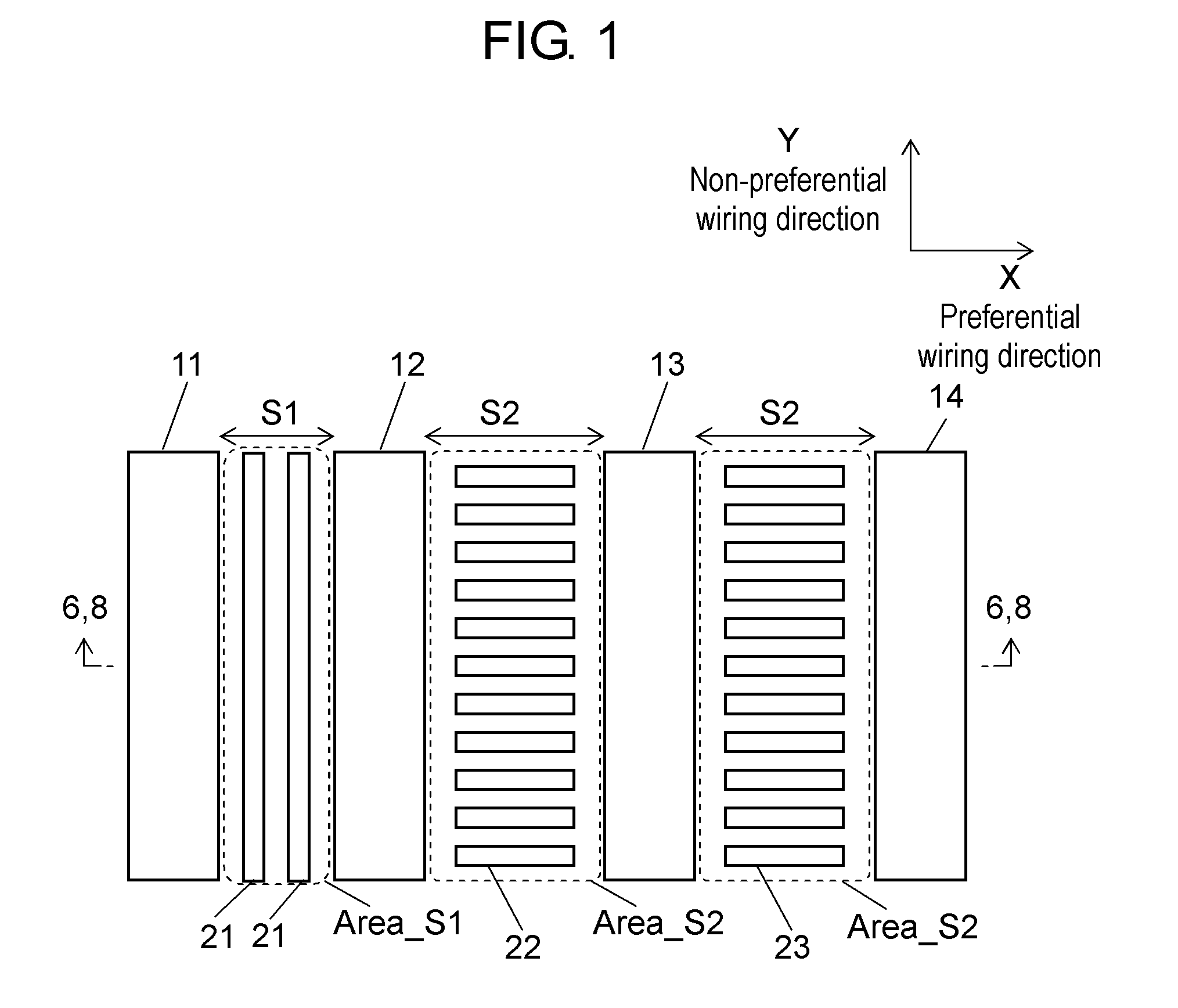
[0028]FIG. 1 is a partial plan view of one wiring layer of a semiconductor device according to a first exemplary embodiment. Active wirings 11, 12, 13, and 14 are formed on wiring layer Mx. These wirings are copper wirings, aluminum wirings, or the like. The spacing between wirings 11 and 12 is S1, and the spacing between wirings 12 and 13 and the spacing between wirings 13 and 14 are S2 (where S12). Wiring voids Area_S1 and Area_S2 defined by spacings S1 and S2, respectively, are dummy pattern formable regions where dummy patterns can be formed. The direction X is a preferential wiring direction of wiring layer Mx, and the direction Y is a non-preferential wiring direction. There is a rule for each wiring layer to preferentially lay out wirings in the vertical or horizontal direction, and the direction of laying out wirings preferentially is a preferential wiring direction. A non-preferential wiring direction is a direction orthogonal to the preferential wiring direction.
[0029]In g...
second exemplary embodiment
[0036]FIG. 4 is a partial plan view of one wiring layer of a semiconductor device according to the second exemplary embodiment. Hereinafter, only the difference from the first exemplary embodiment will be described.
[0037]Wirings 11 to 13 are power supply wirings, and wiring 14 is a signal wiring for transferring clock signals, data signals, or the like. When dummy patterns are disposed near a signal wiring, the interwiring capacitance increases, which decreases signal transfer speed or increases power consumption. Therefore, it is preferable to separate dummy patterns from a signal wiring as much as possible. Specifically, the dummy patterns are separated from the signal wiring by a spacing of S_SIG2 (where, S_SIG2>S_SIG) or more. As a result, dummy pattern 25 extending in the non-preferential wiring direction is formed in a dummy pattern formable region between wirings 13 and 14. When wiring 11 is a signal wiring, the number of dummy patterns 21 in wiring void Area_S1 between wirin...
third exemplary embodiment
[0040]FIG. 6 is a partial cross-sectional view of a semiconductor device according to the third exemplary embodiment and is a cross-sectional view taken along the line 6-6, of a portion including wirings 11 and 12 of the semiconductor device shown in FIG. 1. Hereinafter, only the difference from the first embodiment will be described.
[0041]Wiring layers Mx+1 and Mx−1 in which a plurality of wirings 101 extending in the non-preferential wiring direction of wiring layer Mx is formed are disposed right above and below wiring layer Mx. In these upper and lower wiring layers, region 102 which overlaps dummy pattern 21 formed in wiring layer Mx in a plan view thereof is a non-wiring formation region where no wiring is formed. That is, in the upper and lower wiring layers, no active wiring is formed in the region which overlaps dummy pattern 21 in a plan view. Alternatively, dummy pattern 21 is not formed in a region of the upper and lower wiring layers, which overlaps a wiring formation r...
PUM
 Abstract
Description
Claims
Application Information