

Light emitting device, display apparatus, and electronic apparatus
- Summary
- Abstract
- Description
- Claims
- Application Information
AI Technical Summary
Benefits of technology
Problems solved by technology
Method used
Image

Examples
first embodiment
Overview of Display Apparatus
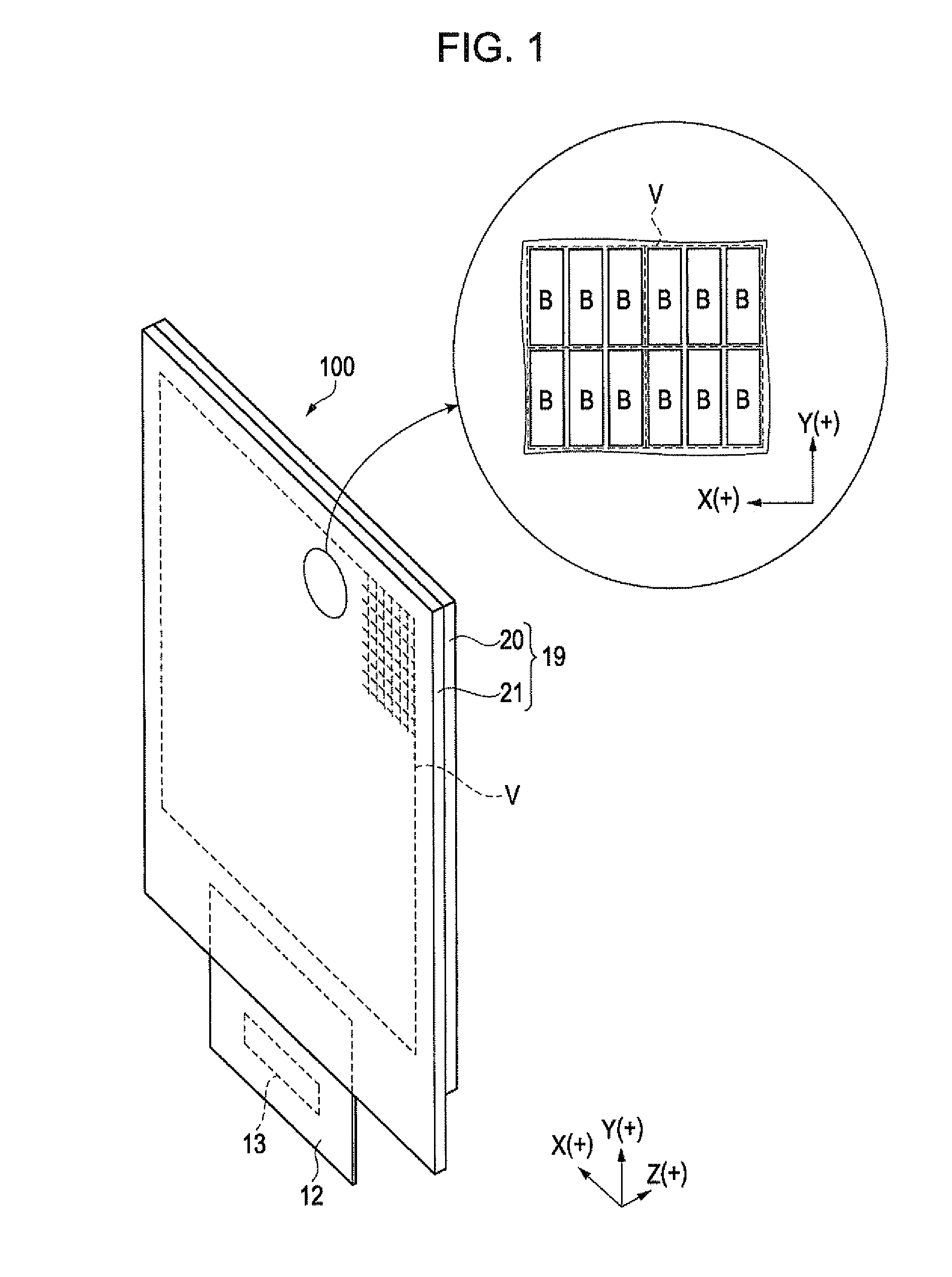
[0051]FIG. 1 is a perspective diagram illustrating an aspect of a display apparatus according to an embodiment.
[0052]First, overview of a display apparatus as the display apparatus according to the first embodiment of the invention is described.
[0053]The display apparatus 100 is an organic EL display apparatus and includes a display panel 19, a flexible board 12, and the like. The display panel 19 is a bottom emission type organic EL display panel where a functional layer including a light-emitting layer is interposed between a substrate 21 and a sealing substrate 20 and emits display light from the substrate 21 side.
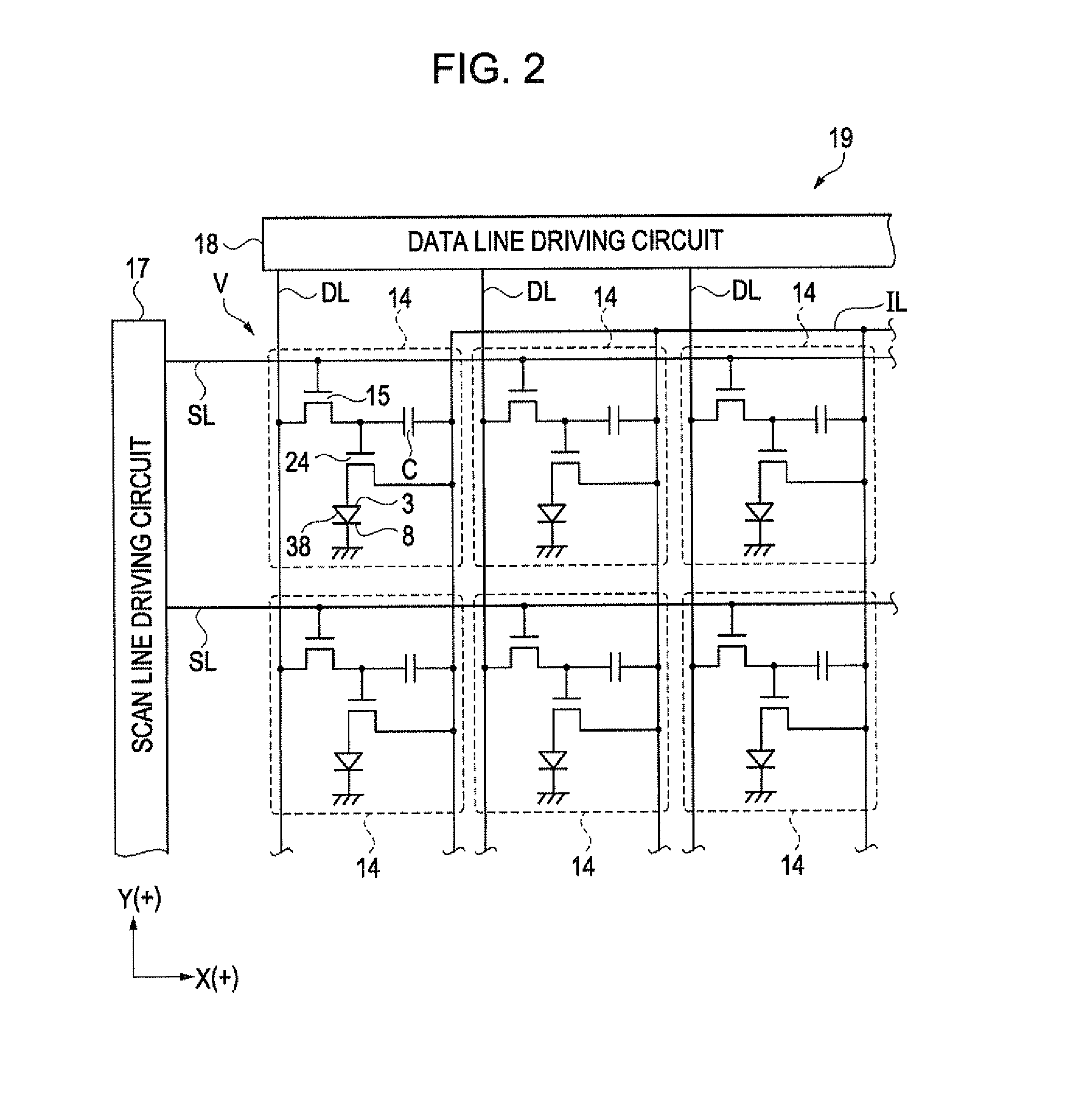
[0054]The display panel 19 has a display area V where a plurality of pixels are disposed in a matrix shape. As enlarged and illustrated in the upper right portion of FIG. 1, in the display area V, blue (B) pixels are arranged, so that a blue monochromic image is displayed by display light emitted from the pixels. In addition, each of the pix...
second embodiment
Overview of Display Apparatus
[0154]FIG. 2 is a perspective diagram illustrating an aspect of a display apparatus according to an embodiment and corresponds to FIG. 1.
[0155]First, overview of a display apparatus as the display apparatus according to the second embodiment of the invention is described. In addition, the same components as those of the first embodiment are indicated by the same reference numerals, and the description thereof is omitted.
[0156]The display apparatus 110 according to the embodiment includes a display panel 29 capable of displaying a full color image. More specifically, as illustrated in the enlarged diagram of the display area V in the upper right portion of FIG. 4, the display apparatus 110 includes a display panel 29 where red (R), green (G), and blue (B) pixels are periodically formed. The other configurations are the same as those of the display apparatus 100 according to the first embodiment.
Details of Light Emitting Device
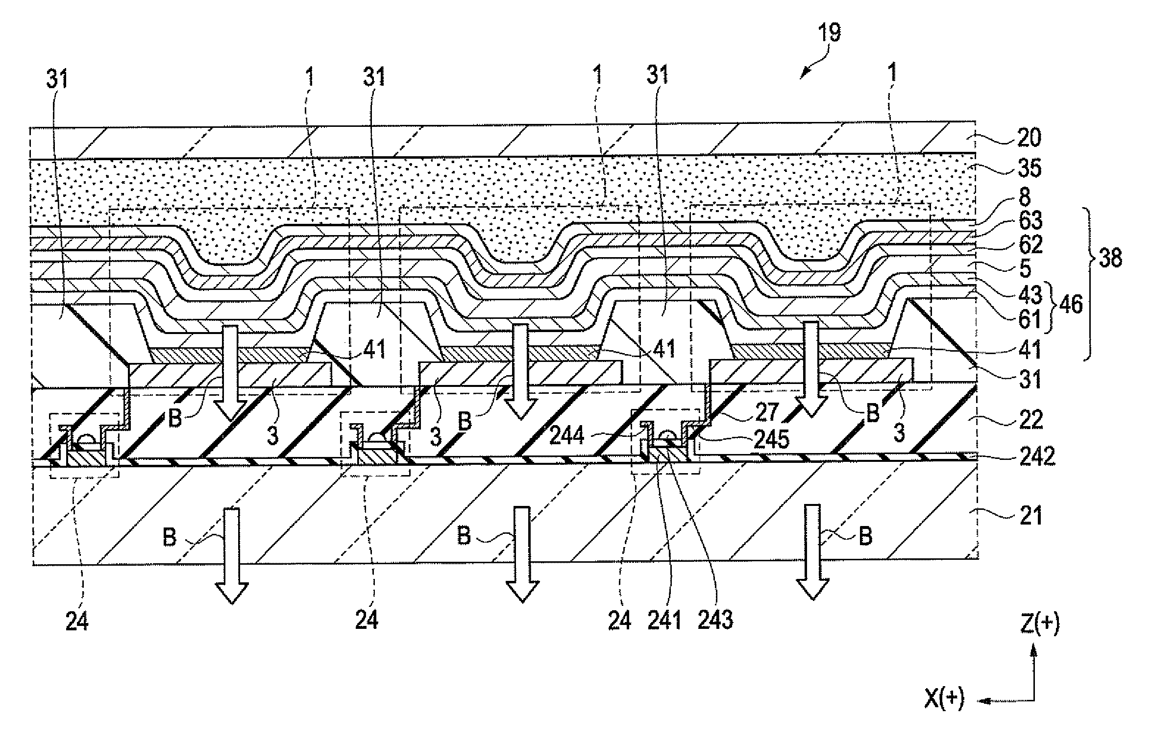
[0157]FIG. 5 is a side cross-...
third embodiment
Electronic Apparatus
[0279]FIG. 8 is a perspective diagram illustrating a configuration of a mobile type (or notebook type) personal computer as an electronic apparatus according to the invention.
[0280]The aforementioned display apparatus 100 (110) of the embodiments may be assembled in various types of the electronic apparatuses.
[0281]In FIG. 8, a personal computer 1100 is configured to include a main body unit 1104 having a keyboard 1102 and a display unit 1106 having a display portion. The display unit 1106 is rotatably supported through a hinge structure member with respect to the main body unit 1104.
[0282]In the personal computer 1100, the display portion included in the display unit 1106 is configured as the aforementioned display apparatus 100 (110).
[0283]FIG. 9 is a perspective diagram illustrating a configuration of a mobile phone (including PHS) as an electronic apparatus according to the invention.
[0284]In FIG. 9, a mobile phone 1200 is configured to include a plurality of...
PUM
 Abstract
Description
Claims
Application Information