Thermal Conduction Paths for Semiconductor Structures

a technology of conduction paths and semiconductors, applied in semiconductor devices, semiconductor/solid-state device details, electrical devices, etc., can solve the problems of extreme heat generation density of circuitry, significant problems in terms of the thermal performance of soi technology, and significant problems in terms of the device's ability to dissipate hea

Active Publication Date: 2012-06-14
QUALCOMM INC
View PDF10 Cites 153 Cited by
  • Summary
  • Abstract
  • Description
  • Claims
  • Application Information

AI Technical Summary

Problems solved by technology

However, as described below the insulator layer that is the source of this advantageous aspect creates significant problems in terms of the thermal performance of SOI technology.
However, the introduction of the insulator layer (e.g. 102) creates a significant problem in terms of the device's ability to dissipate heat.
In modern integrated circuits, the heat generation density of circuitry can be extreme.
The nearly 100-fold reduction in heat dissipation performance exhibited by SOI technology is highly problematic.
A high level of heat in an integrated circuit can shift the electrical characteristics of its devices outside an expected range causing critical design failures.
Left unchecked, excess heat in a device can lead to permanent and critical failures in the form of warping or melting of materials in the device's circuitry.
The dissipation of heat in layer transferred structures poses a significant problem.
Lateral heat conduction is extremely difficult in SOI and layer transferred devices.
Producing thicker layers is more costly in terms of the time it takes to deposit, grow or implant the layer.
Since the production of semiconductor structures requires the use of extremely expensive capital equipment, procedures that take large amounts of time are prohibitively expensive.
Thicker layers also introduce complexity into the process because planarization is more difficult with thicker layers.

Method used


Image

  • Thermal Conduction Paths for Semiconductor Structures
  • Thermal Conduction Paths for Semiconductor Structures
  • Thermal Conduction Paths for Semiconductor Structures

Examples


Embodiment Construction

[0017]Reference now will be made in detail to embodiments of the disclosed invention, one or more examples of which are illustrated in the accompanying drawings. Each example is provided by way of explanation of the present technology, not as a limitation of the present technology. In fact, it will be apparent to those skilled in the art that modifications and variations can be made in the present technology without departing from the spirit and scope thereof. For instance, features illustrated or described as part of one embodiment may be used with another embodiment to yield a still further embodiment. Thus, it is intended that the present subject matter covers all such modifications and variations within the scope of the appended claims and their equivalents.

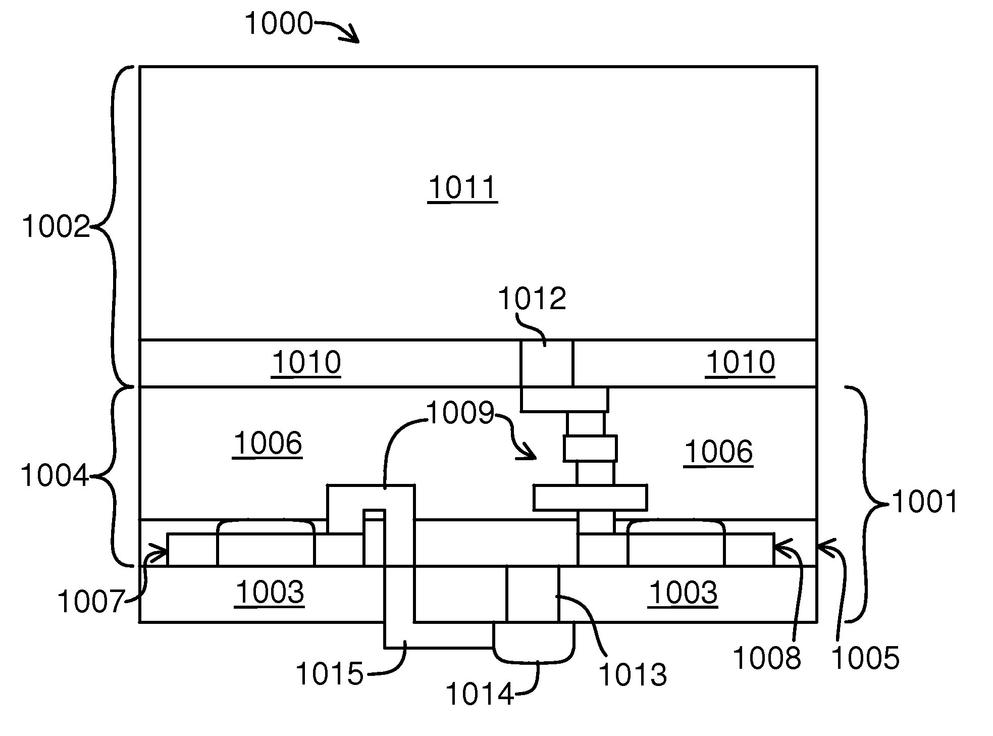
[0018]Embodiments of the present invention provide thermal paths that act as heat sinks for the active circuitry in semiconductor-on-insulator (SOI), bulk semiconductor and layer transferred semiconductor structures. In some ...


PUM


Abstract

A thermal path is formed in a layer transferred semiconductor structure. The layer transferred semiconductor structure has a semiconductor wafer and a handle wafer bonded to a top side of the semiconductor wafer. The semiconductor wafer has an active device layer formed therein. The thermal path is in contact with the active device layer within the semiconductor wafer. In some embodiments, the thermal path extends from the active device layer to a substrate layer of the handle wafer. In some embodiments, the thermal path extends from the active device layer to a back side external thermal contact below the active device layer.

Description

CROSS-REFERENCE TO RELATED APPLICATIONS[0001]This patent document claims priority to Provisional Patent Application No. 61 / 422,650 filed Dec. 13, 2010, under 35 U.S.C. §119(e), which is incorporated herein by reference in its entirety.BACKGROUND OF THE INVENTION[0002]Semiconductor-on-insulator (SOI) technology, which represents an advance over traditional bulk semiconductor processes, was first commercialized in the late 1990s. The defining characteristic of SOI technology is that the semiconductor region in which circuitry is formed is isolated from bulk substrate by an electrically insulating layer.[0003]As used herein and in the appended claims, the region in which signal-processing circuitry is formed on an SOI structure is referred to as the active layer of the SOI structure. When reference is made particularly to the layer of active semiconductor material that forms the active devices in an SOI structure the term active device layer is used instead.[0004]The insulating layer o...

Claims


Application Information

Patent Timeline
Patent Type & Authority Applications(United States)
IPC IPC(8): H01L23/34H01L21/30
CPCH01L23/36H01L23/3677H01L2924/09701H01L2924/0002H01L2924/00
Inventor STUBER, MICHAEL A.BRINDLE, CHRISMOLIN, STUART B.
Owner QUALCOMM INC
Why Eureka
Try Eureka