High power leds with non-polymer material lenses and methods of making the same

a technology of non-polymer material and leds, which is applied in the manufacture of semiconductor/solid-state devices, semiconductor devices, electrical apparatus, etc., can solve the problems of lens heat-up, certain undesirable effects, and the polymer material of the lens to degrade more quickly, so as to avoid damage to the metalized part and high bonding or mounting temperature

Active Publication Date: 2012-06-21
CREELED INC
View PDF2 Cites 20 Cited by
  • Summary
  • Abstract
  • Description
  • Claims
  • Application Information

AI Technical Summary

Benefits of technology

[0011]The present invention is generally directed to LED chips and packages having lenses made of materials that resist degradation at higher operation temperatures and/or high humidity, and methods of fabricating the sam

Problems solved by technology

However, high temperatures from the highly driven LEDs can spread to the lens, causing the lens heat-up.
This can cause the polymer material of the lenses to degrade more quickly than would typically occur with operation under lower temperatures, and this degradation can result in certain undesirable effects for the LED package.
In some cases the lens can become discolored or browned or even cracked, which can significantly reduce the transparency of the lens and can result in absorption of LED light passing through the lens.
This in turn can reduce the overall emission efficiency of the package.
This discoloration can also result in a shift in the color of light emit

Method used


Image

  • High power leds with non-polymer material lenses and methods of making the same
  • High power leds with non-polymer material lenses and methods of making the same
  • High power leds with non-polymer material lenses and methods of making the same

Examples


Embodiment Construction

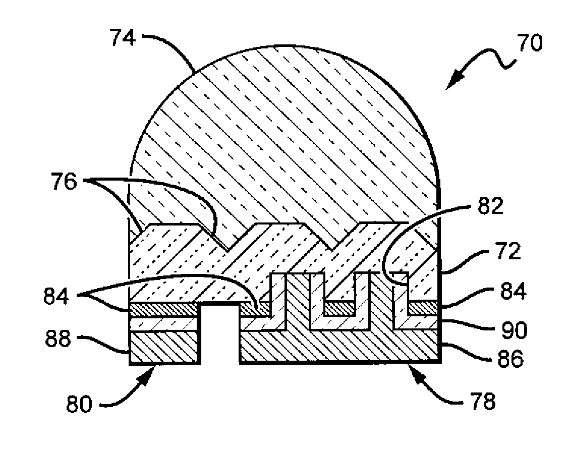
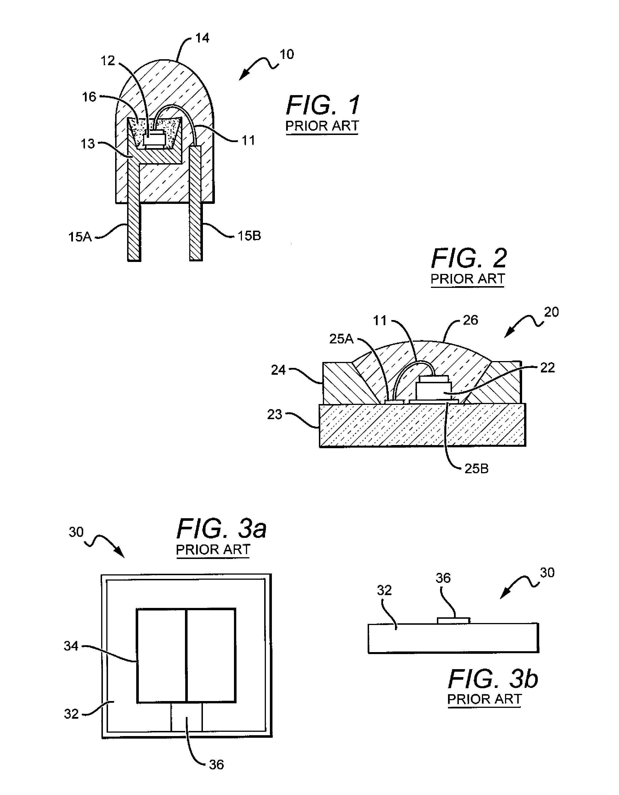
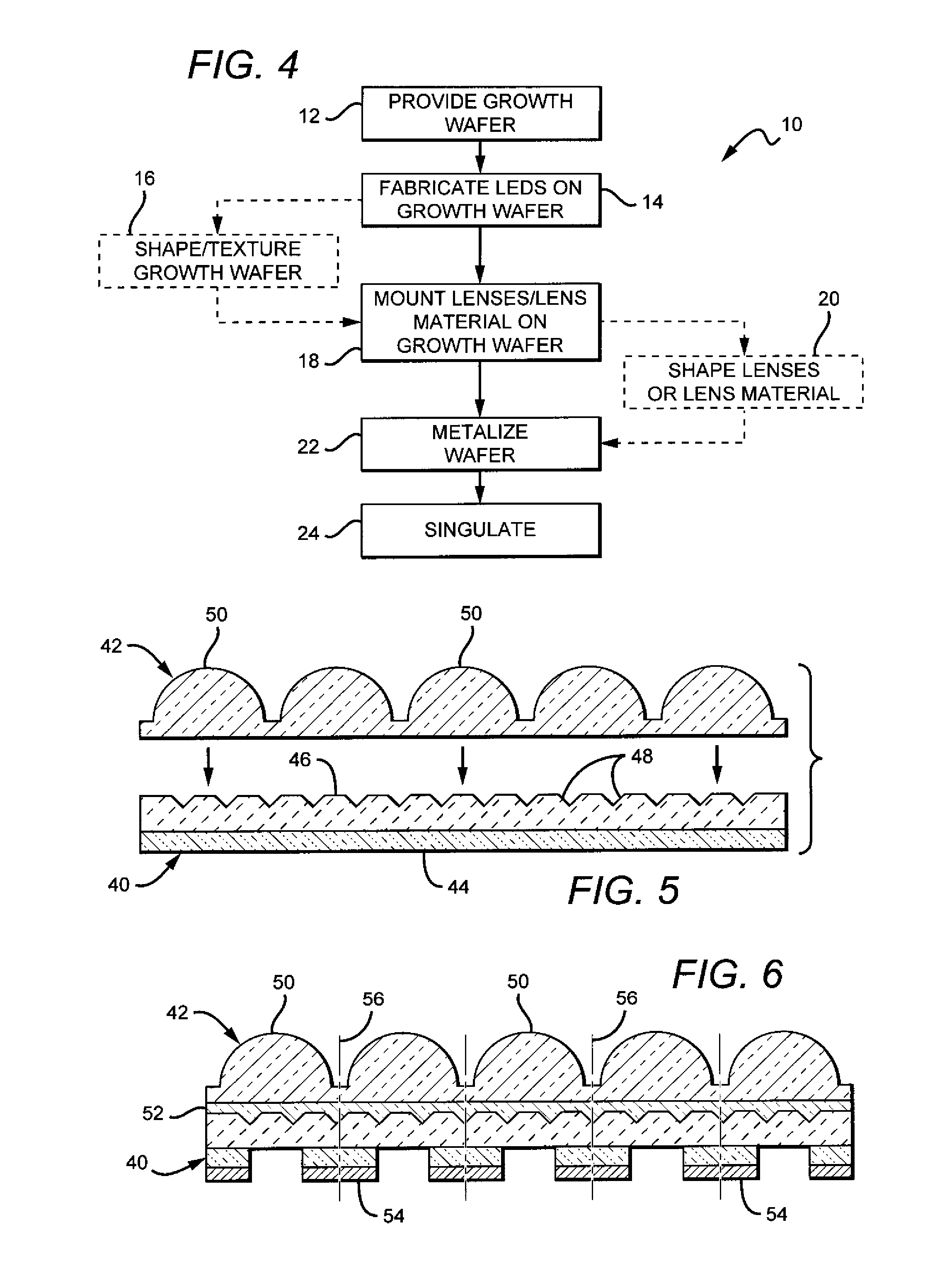
[0030]The present invention is directed to LED chips and LED packages, and methods for fabrication of the same. In particular, the present invention is directed to LED chips and LED packages (“LED chip” or “LED chips”) fabricated having lenses (or encapsulants) that withstand degradation from environmental conditions such as elevated temperatures. The lenses can be made of many different materials that can have some or all of the following characteristics. The material should be substantially transparent to the light emitted by the LED chip and the light converted by wavelength converters, and it should maintain its transparency over time, even when exposed to elevated temperatures and / or high humidity. The material should also have a coefficient of thermal expansion (CTE) that is similar to that of the LED semiconductor material. This allows for reliable operation through different temperature cycles.

[0031]The lens material should also have an index of refraction (IR) that allows f...


PUM


Abstract

LED chips and packages are disclosed having lenses made of materials that resist degradation at higher operation temperatures and humidity, and methods of fabricating the same. The lenses can be made of certain materials that can withstand high temperatures and high humidity, with the lenses mounted to the LED prior to certain critical metallization steps. This helps avoid damage to the metalized part that might occur as a result of the high mounting or bonding temperature for the lens. One embodiment of an LED chip comprises a flip-chip LED and a lens mounted to the topmost surface of the flip-chip LED. Lenses can be bonded to LEDs at the wafer level or at the chip level. The lens comprises a non-polymer material and the LED chip is characterized as having substantially no polymer materials in contact with the LED chip.

Description

BACKGROUND OF THE INVENTION[0001]1. Field of the Invention[0002]This invention relates to light emitting diodes (LED) and in particular LEDs using lenses made of non-polymer materials.[0003]2. Description of the Related Art[0004]Light emitting diodes (LED or LEDs) are solid state devices that convert electric energy to light, and generally comprise one or more active layers of semiconductor material sandwiched between oppositely doped layers. When a bias is applied across the doped layers, holes and electrons are injected into the active layer where they recombine to generate light. Light is emitted from the active layer and from all surfaces of the LED.[0005]In order to use an LED chip in a circuit or other like arrangements, it is known to enclose an LED chip in a package to provide environmental and / or mechanical protection, color selection, light extraction, light focusing and the like. An LED package can also include electrical leads, contacts or traces for electrically connect...

Claims


Application Information

Patent Timeline
IPC IPC(8): H01L33/60H01L33/00H01L33/48
CPCH01L33/58H01L2224/48091H01L2224/48247H01L2224/73265H01L2924/00014H01L2924/181H01L2924/00012H01L27/156H01L33/54
Inventor YAO, ZHIMIN JAMIE
Owner CREELED INC
Why Eureka
Try Eureka