Integrated circuit and semiconductor device
a technology of integrated resistance and integrated circuit, which is applied in the direction of semiconductor devices, diodes, instruments, etc., can solve the problems of increasing the cost of the semiconductor device and the number of externally mounted components, so as to reduce the cost of the semiconductor device and the power supply system using the semiconductor device, the power consumption of the current can be reduced, and the number of external components mounted on the semiconductor device can be reduced.
- Summary
- Abstract
- Description
- Claims
- Application Information
AI Technical Summary
Benefits of technology
Problems solved by technology
Method used
Image
Examples
embodiment 1
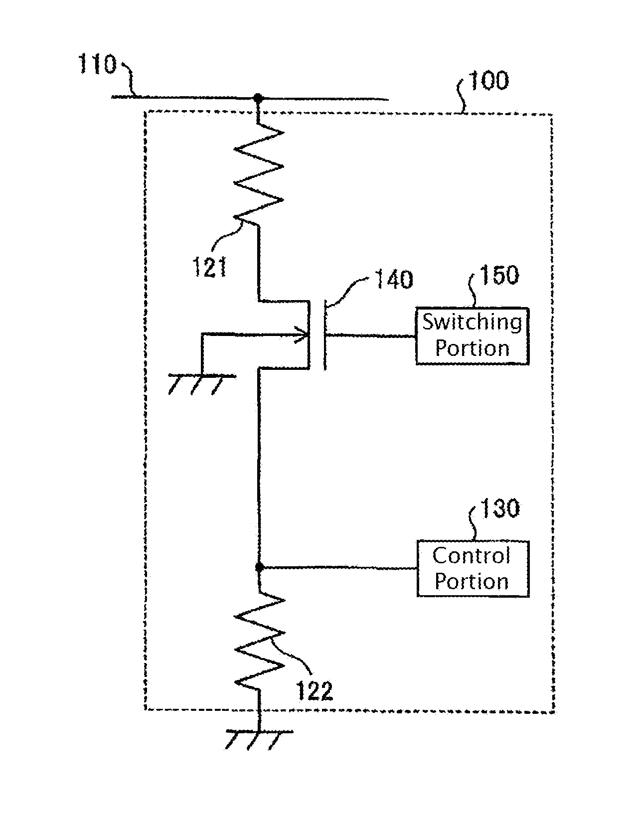
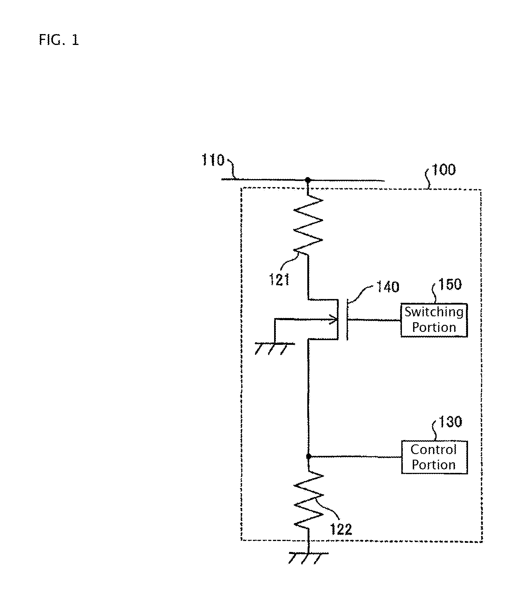
[0140]FIG. 1 is a circuit diagram showing principle portions of the integrated circuit of Embodiment 1 of the invention. As shown in FIG. 1, the integrated circuit 100 of Embodiment 1 comprises a first resistor 121, second resistor 122, control portion 130, switch 140, and switching portion 150. All of these elements are formed on the same semiconductor substrate. A voltage obtained by rectifying an alternating-current voltage, or a direct-current voltage, is input to the integrated circuit 100 from a high-voltage line 110.
[0141]One end of the first resistor 121 is connected to the high-voltage line 110, and the other end of the first resistor 121 is connected to one end of the switch 140. One end of the second resistor 122 is connected to the other end of the switch 140, and the other end of the second resistor 122 is grounded. The first resistor 121 and second resistor 122 form a resistive voltage divider element, which resistively divides a voltage obtained by rectifying an alter...
embodiment 2
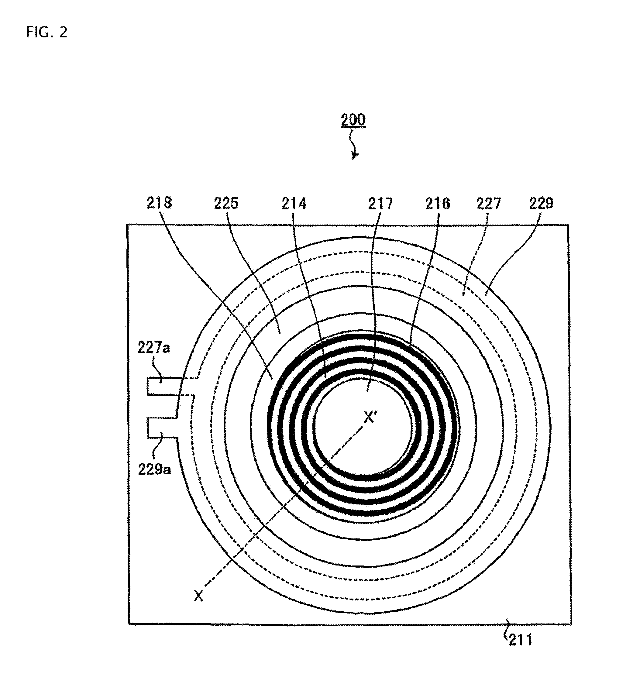
[0190]FIG. 8 is a plane view showing principle portions of the semiconductor device of Embodiment 2 of the invention. Further, FIG. 9 is a cross-sectional view sectioning the semiconductor device shown in FIG. 8 along the section line X-X′. In FIG. 8 and FIG. 9, the same symbols are assigned for the configuration similar to the configuration shown in FIG. 2 and FIG. 3, and explanations are omitted. As shown in FIG. 8 and FIG. 9, in the semiconductor device 200 of Embodiment 2, the high-voltage high-resistance element 216 is formed such that the planar shape thereof is for example a circular ring shape.
[0191]FIG. 10 is a plane view showing a modified example of the semiconductor device shown in FIG. 8. In FIG. 10, the same symbols are assigned for the configuration similar to the configuration shown in FIG. 8, and explanations are omitted. In FIG. 8, all configurations, excepting the P-type semiconductor substrate 211 of the semiconductor device 200, are formed in a planar shape whic...
embodiment 3
[0195]FIG. 13 is a circuit diagram showing principle portions of the integrated circuit of Embodiment 3 of the invention. In FIG. 13, the same symbols are assigned for the configuration similar to the configuration shown in FIG. 1, and explanations are omitted. As shown in FIG. 13, the integrated circuit 100 of Embodiment 3 comprises, in addition to the configuration of the integrated circuit 100 shown in FIG. 1, a third resistor 1421 and fourth resistor 1422, a control portion 1430, second switch 1440, and second switching portion 1450.
[0196]The configurations of the third resistor 1421, fourth resistor 1422, control portion 1430, second switch 1440, and second switching portion 1450 are similar to those of the first resistor 121, second resistor 122, control portion 130, switch 140, and switching portion 150, respectively. The first resistor 121, switch 140, third resistor 1421, and second switch 1440 are configured as an integrally configured semiconductor device 200 (see FIG. 14...
PUM
 Abstract
Description
Claims
Application Information


