Display device

a display device and display technology, applied in static indicating devices, instruments, optics, etc., can solve the problems of deteriorating display quality, increased power consumption, and delay in signal transmission to the end portion of a signal line, so as to reduce parasitic capacitance between the scan line and the first electrode, the effect of reducing the aperture ratio of a pixel

Active Publication Date: 2012-06-21
SEMICON ENERGY LAB CO LTD
View PDF18 Cites 29 Cited by
  • Summary
  • Abstract
  • Description
  • Claims
  • Application Information

AI Technical Summary

Benefits of technology

[0016]A plurality of thin film transistors have the first electrode which serves as the one of the source electrode and the drain electrode, in common. Therefore, the area where the one of the source electrode and the drain electrode and the scan line are overlapped with each other can be reduced, and parasitic capacitance generated between the scan line and the first electrode can be reduced while keeping the aperture ratio of a pixel.
[0017]In addition, part of the scan line has a loop shape including an opening, and the first electrode which serves as the one of the source electrode and the drain electrode in the thin film transistor is located in a r

Problems solved by technology

Further, increase in wiring resistance and parasitic capacitance between wirings causes delay of signal transmission to an end portion of a signal

Method used


Image

  • Display device
  • Display device
  • Display device

Examples


embodiment 1

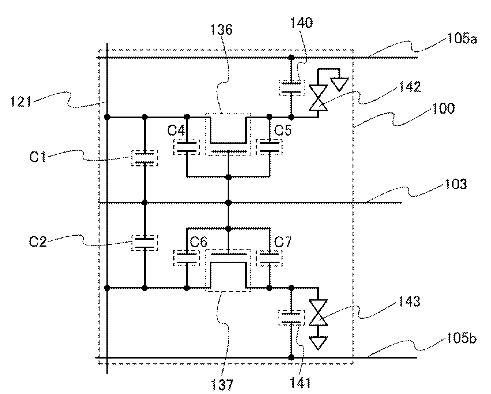
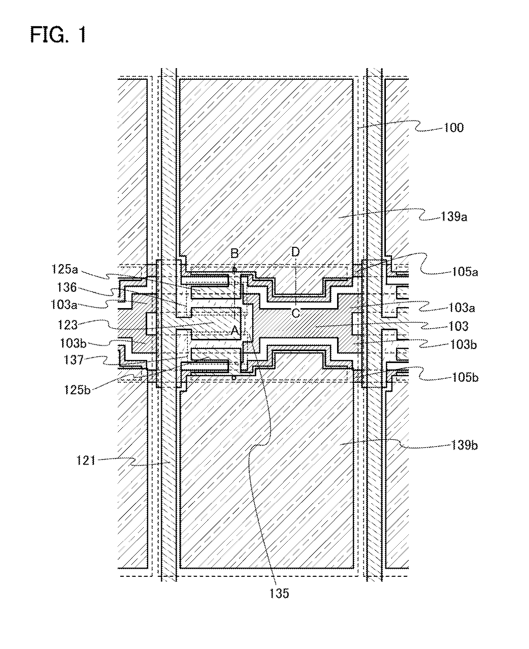
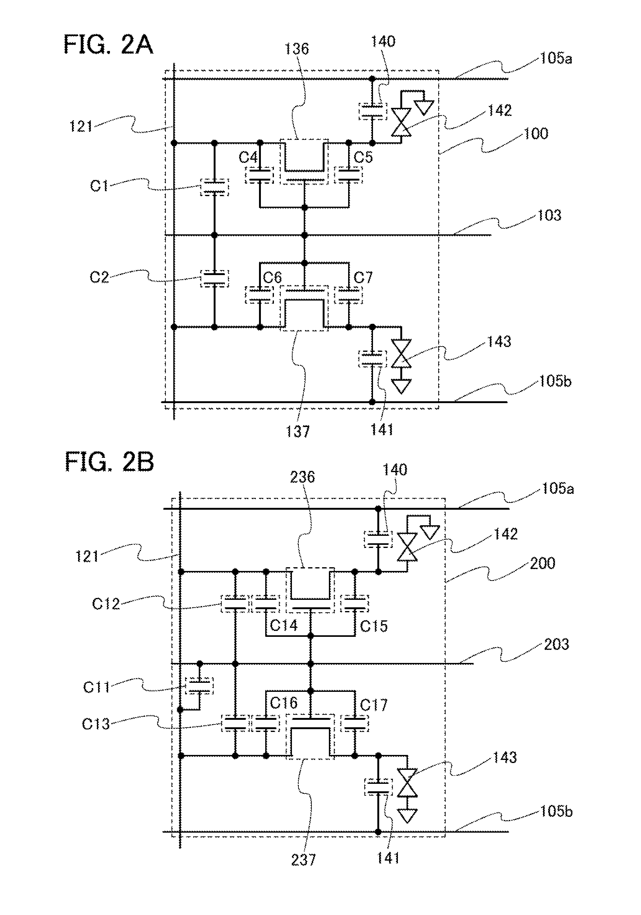
[0029]In this embodiment, a structure of a pixel of a liquid crystal display device in which wiring capacitance is reduced will be described with reference to FIG. 1, FIGS. 2A and 2B, FIGS. 3A and 3B, and FIGS. 8A to 8C. Note that a pixel in which one pixel is provided with a plurality of subpixels is described as a pixel 100 in this embodiment; however, one embodiment of the present invention is not limited thereto.

[0030]FIG. 1 is a top view of the pixel 100 of a multi-domain liquid crystal display device, which is described in this embodiment. FIG. 2A is a circuit diagram of the pixel 100 in FIG. 1. FIG. 2B is a circuit diagram of a conventional pixel. FIG. 3A is a cross-sectional view taken along dashed-and-dotted line A-B in FIG. 1. FIG. 3B is a cross-sectional view taken alone dashed-and-dotted line C-D in FIG. 1. FIG. 8A is an enlarged top view of the vicinity of a thin film transistor 136 and a thin film transistor 137 in FIG. 1. FIG. 8B is a top view illustrating only a scan...

embodiment 2

[0085]In this embodiment, a structure of a pixel, which has a structure different from that in Embodiment 1, of a liquid crystal display device whose wiring capacitance is reduced will be described with reference to FIG. 4 and FIG. 5. Note that a pixel in which one pixel is provided with a plurality of subpixels is described as a pixel 150 in this embodiment; however one embodiment of the present invention is not limited thereto.

[0086]FIG. 4 is a top view of the pixel 150 of a multi-domain liquid crystal display device, which is described in this embodiment, and FIG. 5 is a cross-sectional view taken along dashed-and-dotted line E-F in FIG. 4.

[0087]As illustrated in FIG. 4, the pixel 150 includes the scan line 103; a signal line 151 which intersects with the scan line 103; and the capacitor wiring 105a and the capacitor wiring 105b which extend in the same direction as the scan line 103. The scan line 103 is provided between the capacitor wiring 105a and the capacitor wiring 105b.

[...

embodiment 3

[0112]In this embodiment, a method for manufacturing the thin film transistors described in Embodiments 1 and 2 will be described with reference to FIGS. 6A to 6D and FIGS. 7A and 7B. A method for manufacturing the thin film transistor 136 in Embodiment 1 is described here; however, the method can be applied to the thin film transistor 137 in Embodiment 1 and the thin film transistors 166 and 167 in Embodiment 2 as appropriate. Note that an n-channel thin film transistor has higher carrier mobility than a p-channel thin film transistor. Further, it is preferable that all thin film transistors formed over the same substrate have the same polarity because the number of manufacturing steps can be reduced. Therefore, in this embodiment, a method for manufacturing an n-channel thin film transistor is described.

[0113]As illustrated in FIG. 6A, the scan line 103 is formed over the substrate 101. Next, the gate insulating film 107 which covers the scan line 103 is formed, and a microcrystal...


PUM


Abstract

To provide a display device in which parasitic capacitance between wirings can be reduced while preventing increase in wiring resistance. To provide a display device with improved display quality. To provide a display device with low power consumption. A pixel of the liquid crystal display device includes a signal line, a scan line intersecting with the signal line, a first electrode projected from the signal line, a second electrode facing the first electrode, and a pixel electrode connected to the second electrode. Part of the scan line has a loop shape, and part of the first electrode is located in a region overlapped with an opening of the scan line. In other words, part of the first electrode is not overlapped with the scan line.

Description

BACKGROUND OF THE INVENTION[0001]1. Field of the Invention[0002]The present invention relates to a display device and a method for manufacturing the display device.[0003]2. Description of the Related Art[0004]In recent years, as liquid crystal display devices in which viewing angle characteristics and display quality are improved, vertically aligned (VA) liquid crystal display devices are provided. As VA liquid crystal display devices, a multi-domain liquid crystal display device including one pixel provided with a plurality of pixel electrodes and thin film transistors which are connected to the respective pixel electrodes and control the potentials of the respective pixel electrodes is provided. When one pixel is provided with a plurality of pixel electrodes, liquid crystal alignment can be made different in each pixel electrode; therefore, a multi-domain liquid crystal display device can have a larger viewing angle than those of conventional VA liquid crystal display devices (see...

Claims


Application Information

Patent Timeline
IPC IPC(8): G09G5/00
CPCH01L29/786G02F2001/13606G02F1/136286G02F1/13606G02F1/13439G02F1/134309G02F1/1368G02F1/136295G02F2201/40G02F2201/123G02F1/13629H01L27/1225H01L27/124H01L27/1255G02F1/136213G02F1/136277G02F2202/10G02F2202/103G09G3/3677G09G2330/021H01L29/78669H01L29/7869
Inventor HIROSE, ATSUSHI
Owner SEMICON ENERGY LAB CO LTD
Why Eureka
Try Eureka