
Eureka
For R&D, Eureka makes reading and utilizing patents & technical documents easy.
Eureka AIR
Designed for self-driven R&D workflows. Generate viable solutions, solve complex R&D challenges, empower your innovation with AI.

Eureka Materials
Designed for material experts only. Revolutionize your material R&D, from search, analyze, to developing new materials.

TechResearch
Generate reliable direction feasibility study reports for your R&D in just a few steps.

TechSeek
Discover and master advanced knowledge NOW. Basics, ideas, possibilities, all at once.

TechMind
As an expert in R&D Theories, TechMind can generates customized viable solutions instantly.

TechRisk
Analyze your overall solution with one click, know your potential R&D risks in advance.

TechMonitor
Get weekly tech updates, stay abreast of the latest tech innovations and key insights.
Method for fabricating light emitting diode chip
- Summary
- Abstract
- Description
- Claims
- Application Information
AI Technical Summary
Problems solved by technology
Method used
Image

Examples
Embodiment Construction
[0008]An embodiment for fabricating an LED chip will now be described in detail below and with reference to the drawings.
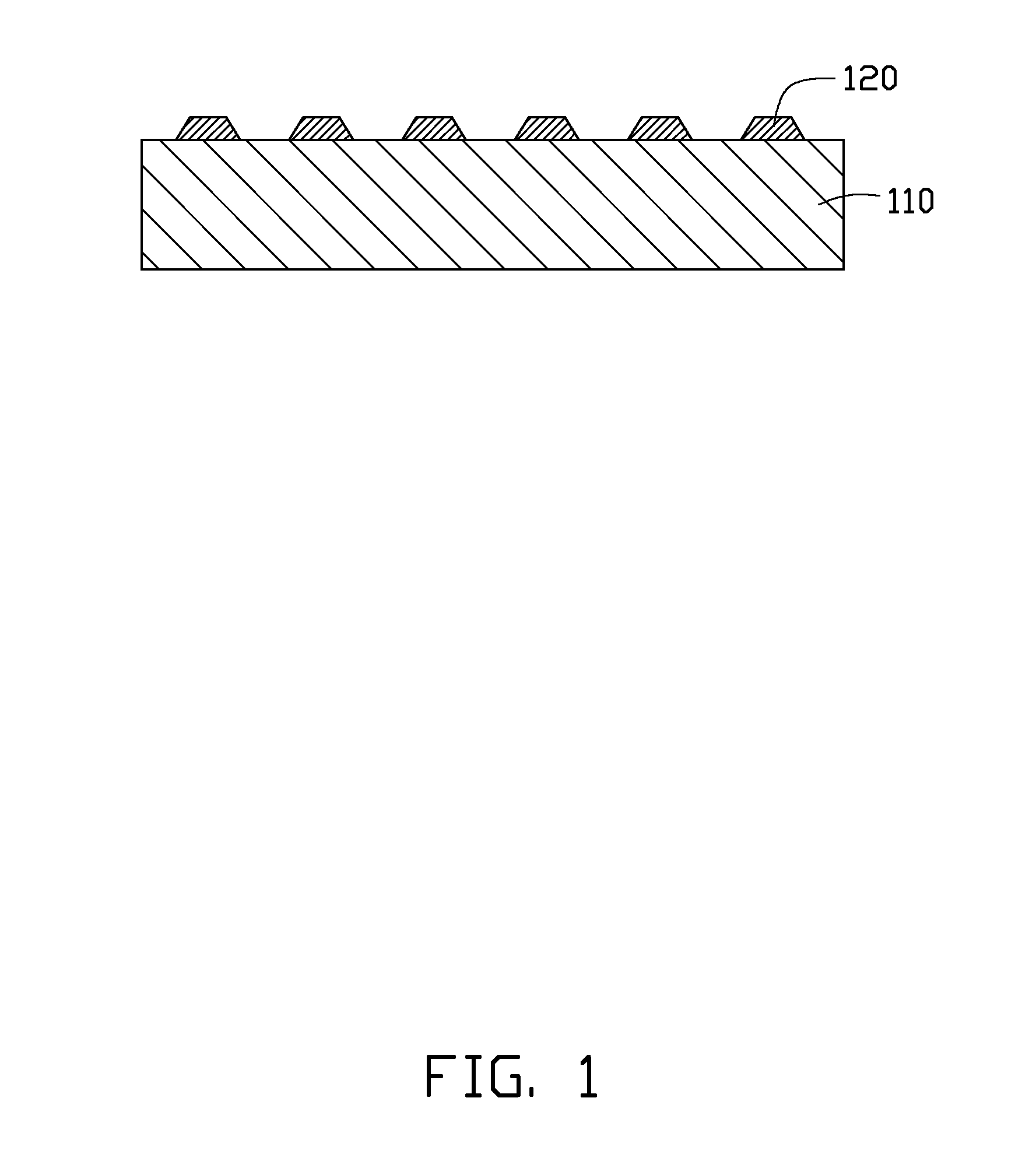
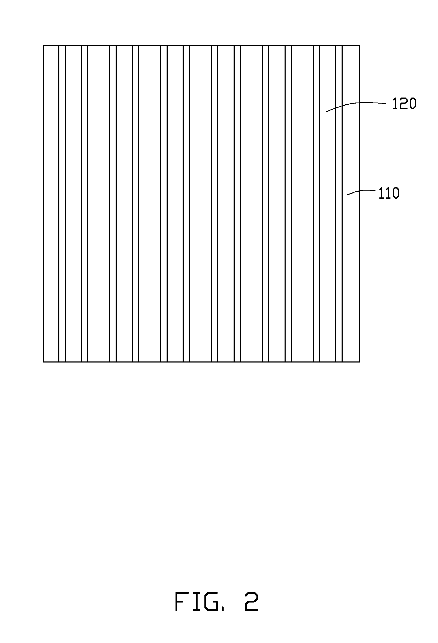
[0009]Referring to FIG. 1, a sapphire substrate 110 is provided, and then a SiO2 pattern layer 120 is formed on the sapphire substrate 110. Further referring to FIG. 2, the SiO2 pattern layer 120 includes a number of SiO2 strips paralleled to each other. Referring also to FIG. 3, a cross section of the SiO2 strips is trapezoid-shaped. In an alternative embodiment, the cross section of the SiO2 strips can be semicircle-shaped.
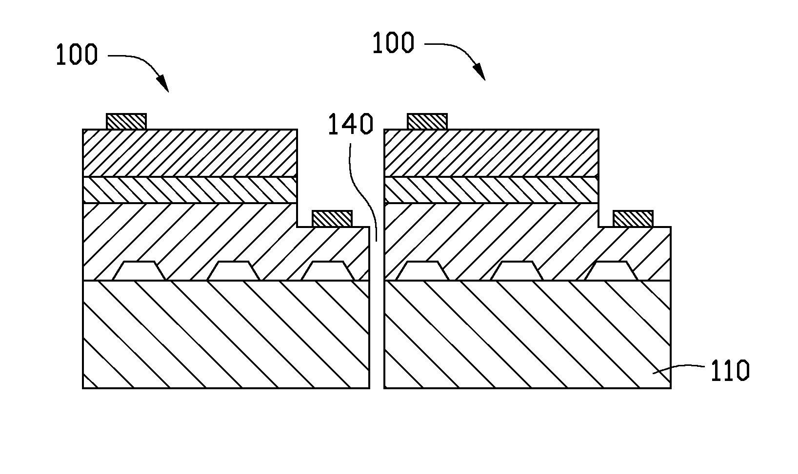
[0010]Referring to FIG. 3, a light emitting structure 130 is formed on an outer surface of the sapphire substrate 110 with the SiO2 pattern layer 120, by metal organic chemical vapor deposition (MOCVD) or molecular beam epitaxy (MBE). The light emitting structure 130 includes a n-type GaN layer 131, a multiple quantum well (MQW) layer 132 and a p-type GaN layer 133 formed subsequently in a direction away from the sapphire substrate 110.
[0011]R...
PUM
 Abstract
Description
Claims
Application Information
 - R&D Engineer
- R&D Manager
- IP Professional
- Industry Leading Data Capabilities
- Powerful AI technology
- Patent DNA Extraction
Browse by: Latest US Patents, China's latest patents, Technical Efficacy Thesaurus, Application Domain, Technology Topic, Popular Technical Reports.
© 2024 PatSnap. All rights reserved.Legal|Privacy policy|Modern Slavery Act Transparency Statement|Sitemap|About US| Contact US: help@patsnap.com