Method for manufacturing a nitride semiconductor device and device manufactured by the method

a technology of nitride and semiconductor devices, which is applied in the direction of semiconductor devices, semiconductor lasers, lasers, etc., can solve the problems of insufficient substrate material, difficult to form a large crystal of gan, and inability to produce a single crystal film of light emitting elements of higher quality

Inactive Publication Date: 2003-04-29
SHOWA DENKO KK
View PDF6 Cites 77 Cited by
  • Summary
  • Abstract
  • Description
  • Claims
  • Application Information

AI Technical Summary

Problems solved by technology

However, it is very difficult to form a large crystal of GaN.
At the higher temperature, semiconductor crystal such as gallium arsenide (GaAs) is unstable so that it is not a proper material for a substrate.
However, the direct growth of GaN on a sapphire substrate can not produce a higher-quality single-crystal film for a light emitting element, because sapphire has a lattice constant different from that of GaN by approximately 14%.
Though a light emitting efficiency characteristic of GaN is less affected by the dislocation density, compared to that of

Method used


Image

  • Method for manufacturing a nitride semiconductor device and device manufactured by the method
  • Method for manufacturing a nitride semiconductor device and device manufactured by the method
  • Method for manufacturing a nitride semiconductor device and device manufactured by the method

Examples


Embodiment Construction

The present invention will be described in conjunction with a preferred embodiment, referring to the accompanying drawings.

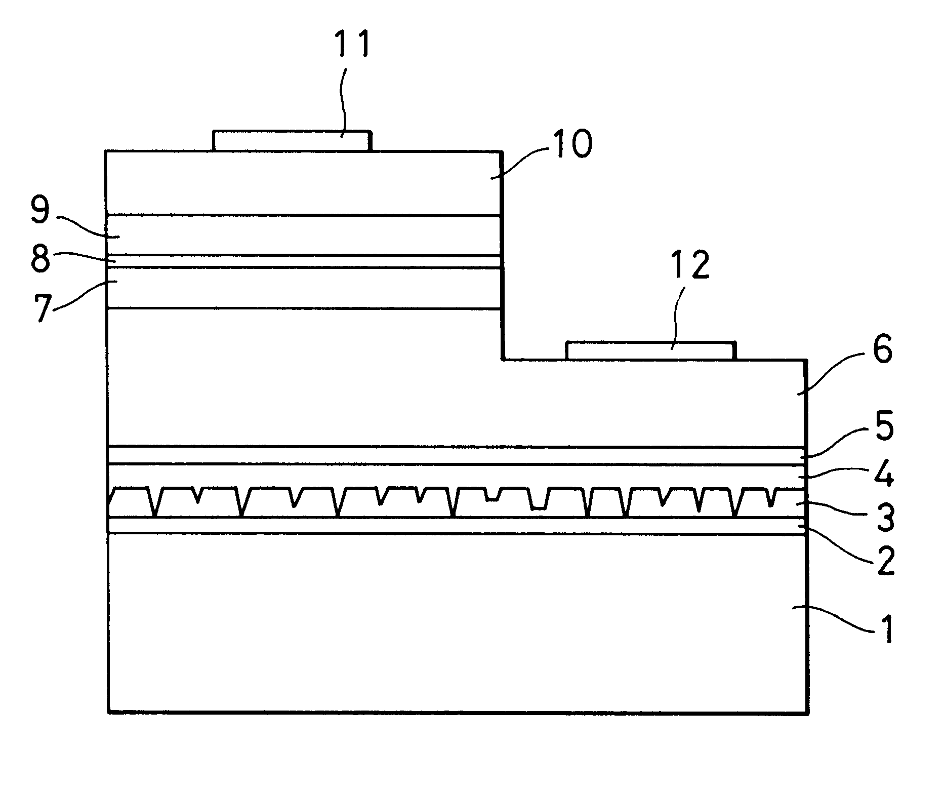
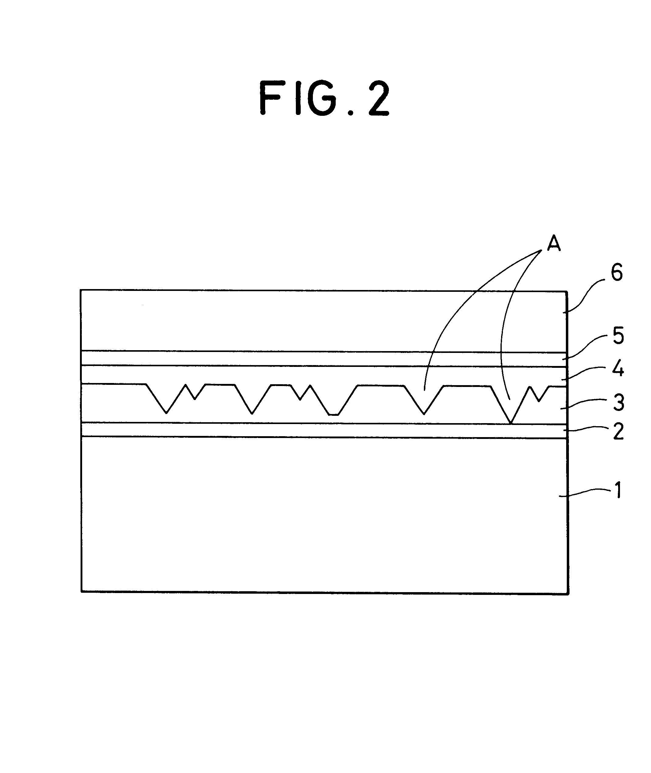
As shown in FIG. 1, a nitride semiconductor device according to the present invention comprises a multilayer structure in which nitride semiconductor single-crystal layers are formed on a sapphire substrate 1. A low temperature buffer layer 2 of AlN or GaN is formed on the sapphire substrate 1. A non-doped GaN crystal layer 3 is formed on the low-temperature buffer layer 2 as a first GaN layer. The non-doped GaN crystal layer 3 takes on an island-like structure without any dopant. A second GaN layer 4 containing a dopant is formed on the first GaN layer. The second GaN layer 4 is deposited while filling pyramidal surface voids in the first GaN layer 3 and flattening the surface of the GaN layer 3.

Moreover, a non-doped GaN crystal film 5 is formed on the second GaN layer 4 as a third GaN layer. Further, a crystal layer 6 is formed on the layer 5. In this embodime...


PUM


Abstract

A group III nitride semiconductor device is disclosed which has a reduced number of threading dislocations adversely affecting characteristics of the group III nitride semiconductor device. A method for manufacturing the group III nitride semiconductor device controls pit formation in a GaN layer formed on a sapphire substrate.First, a low temperature buffer layer is formed on a sapphire substrate by MOCVD. An undoped GaN layer having a predetermined thickness is then grown on the low temperature buffer layer. Next, a GaN layer containing magnesium as a dopant is formed on the layer at a lower pressure than that of depositing the GaN layer, which results in filling pits generated on the GaN layer to flatten the surface of another GaN layer.

Description

1. Field of the InventionThe present invention relates to a method for manufacturing a group III nitride semiconductor device.2. Prior ArtExtensive researches is now underway on nitride-gallium and related compound semiconductor as a material system for short wavelength light emitting devices, in particular short wave length semiconductors lasers. A semiconductor laser device is manufactured by forming a semiconductor single-crystal film on a crystal substrate. Characteristics of a light emitting device as a laser device are greatly dependent on the density of crystal defects in the single-crystal film. From this point of view, the substrate is preferable to be made of a material having the physical-property constants such as crystal structure, lattice constant, and thermal-expansion coefficient the same as those of a semiconductor crystal to be expitaxially grown on the substrate. For example, it is ideal to use a single crystal of gallium nitride (hereinafter referred to as GaN), ...

Claims


Application Information

Patent Timeline
IPC IPC(8): H01S5/323H01L33/00H01S5/00H01L33/12H01L33/32
CPCH01L21/0242H01L21/02458H01L21/02502H01L21/0254H01L21/02579H01L33/12H01L33/32H01S5/32341H01L21/0262H01S2304/04H01L33/007
Inventor WATANABE, ATSUSHITANAKA, TOSHIYUKIOTA, HIROYUKI
Owner SHOWA DENKO KK
Why Eureka
Try Eureka