Semiconductor device

Inactive Publication Date: 2002-04-25
NEC CORP
View PDF0 Cites 79 Cited by
  • Summary
  • Abstract
  • Description
  • Claims
  • Application Information

AI Technical Summary

Problems solved by technology

When a device is manufactured making use of a GaN based semiconductor material, because it is difficult to obtain a bulk GaN based substrate, there is normally employed a method of fabricating a device wherein a GaN based semiconductor layer is formed by epitaxial growth on a substrate of a different material.
SiC has an excellent thermal conductivity but also drawbacks of high cost and difficulty to attain a large wafer area.
First, attempts to obtain a wafer with a larger diameter are limited to a certain extent. In recent years, from the point of view of improving productivity, there have been demands that wafers should have larger diameters. Yet, the sapphire whose C plane is chosen for the crystal growth plane cannot be readily made to have a larger diameter, because of its low workability through surface polishing due to its poor mechanical processing feasibility and little ability to grow the crystal to have a large width by the ribbon crystal method or the like. A substrate with the largest diameter attained so far is 4 inches in diameter.
Secondly, a heat radiation characteristic thereof is difficult to improve. Since sapphire has a low thermal conductivity, improvements on

Method used


Image

  • Semiconductor device
  • Semiconductor device
  • Semiconductor device

Examples


example 1

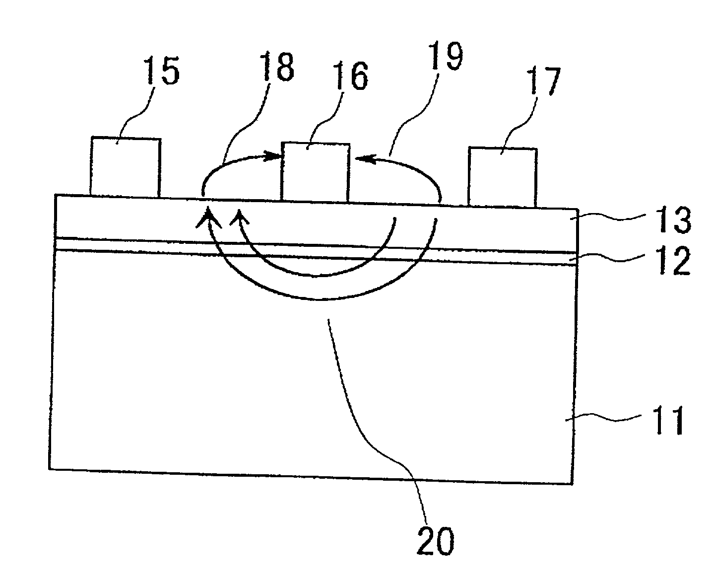
[0093] FIG. 1 shows the structure of an AlGaN / GaN hetero junction FET of the present example. This FET was fabricated by a process which comprises the steps of growing a gallium nitride semiconductor layer upon an A plane sapphire substrate (the basal plane thereof is a (11-20) plane) with a diameter of 8 inches, forming electrodes and so on, and thereafter polishing to a thickness of 30 .mu.m and then breaking into chips.

[0094] A manufacturing method was the similar one to that mentioned in DETAILED DESCRIPTION OF THE INVENTION above. An annealing after cleaning of the substrate was performed in oxygen at 1200.degree. C. The growth temperature for a low-temperature buffer layer was set at about 650.degree. C., and for other layers at about 1050.degree. C., respectively. An epitaxial layer 12 was made to have a structure wherein the following layers were laid in this order: that is

[0095] an AlN buffer layer (with a thickness of 100 .mu.m);

[0096] a GaN layer (with a thickness of 0.5 ...

reference example 1

[0111] Subjecting a HEMT shown in FIG. 8 to analysis where a GaN based semiconductor layer 81 is formed upon a sapphire substrate 80 and a source electrode 82, a gate electrode 83 and a drain electrode 84 are formed thereon, the dependences of thermal resistance and surface average temperature on substrate thickness were obtained by simulation. The calculated results are shown in FIG. 7. The thermal resistance and surface average temperature each decrease with decreasing the substrate thickness, and show a marked decrease, especially in the region of thickness of 50 .mu.m or less. These results confirm that, by setting the thickness of the sapphire substrate to be 50 .mu.m or less, a noticeable effect to heat radiation can be attained.

reference example 2

[0112] A sapphire substrate with a thickness of 300 .mu.m wherein an A plane was set to be the basal plane and another sapphire substrate with a thickness of 300 .mu.m wherein a C plane was set to be the basal plane were prepared, and, after grinding, close inspection of their aspects were conducted. In the sapphire substrate wherein a C plane was set to be the basal plane, cracks appeared when its thickness became 70 .mu.m or so. In contrast with this, in the sapphire substrate wherein an A plane was set to be the basal plane, cracks did not appear, even when the substrate thickness became as thin as 30 .mu.m, showing nothing abnormal in appearance.

Summary of Disclosure

[0113] As set forth above, in the present invention, upon an A plane of a single sapphire substrate, a group III nitride semiconductor layer is formed to construct a FET. This makes it possible to provide a good productivity as well as to improve heat radiation characteristic. Further, as the layout in plane of the F...


PUM


Abstract

An object of the present invention is to improve, in a group III nitride semiconductor device, the productivity, heat radiation characteristic and performance in the element high speed operation; upon a sapphire substrate in which an A plane (an (11-20) plane) is set to be the basal plane, an epitaxial growth layer of a group III nitride semiconductor is formed and, thereon, a gate electrode 16, a source electrode 15 and a drain electrode 17 are formed; these electrodes are disposed in such a way that a direction along which they are laid makes an angle within 20° with respect to a C axis of sapphire.

Description

[0001] The present invention relates to a field effect transistor (FET) with a sapphire substrate, in particular to a field effect transistor utilizing a group III nitride semiconductor material such as GaN.BACKGROUND TO THE INVENTION[0002] The group III nitride semiconductors including GaN have carrier transport characteristics close to that of GaAs, together with high breakdown electric fields due to their wide band gaps. They are, thus, regarded as strong candidate materials for high frequency, high power transistors.[0003] When a device is manufactured making use of a GaN based semiconductor material, because it is difficult to obtain a bulk GaN based substrate, there is normally employed a method of fabricating a device wherein a GaN based semiconductor layer is formed by epitaxial growth on a substrate of a different material. For the substrate of a different material, sapphire or SiC is utilized. SiC has an excellent thermal conductivity but also drawbacks of high cost and di...

Claims


Application Information

Patent Timeline
IPC IPC(8): H01L21/205H01L21/338H01L29/201H01L29/04H01L29/20H01L29/778H01L29/812
CPCH01L29/045H01L29/812H01L29/2003
Inventor OHNO, YASUOHAYAMA, NOBUYUKIKASAHARA, KENSUKENAKAYAMA, TATSUOMIYAMOTO, HIRONOBUTAKAHASHI, YUJIANDO, YUJIMATSUNAGA, KOHJIKUZUHARA, MASAAKI
Owner NEC CORP
Why Eureka
Try Eureka