

Group III nitride semiconductor substrate and its manufacturing method
a technology of nitride semiconductor and substrate, which is applied in the direction of polycrystalline material growth, chemically reactive gas growth, crystal growth process, etc., can solve the problems of substrate warpage caused by the difference in lattice constant and thermal expansion coefficient, easy cracking therein, and difficult uniform adjustment of focus over the whole surface of the substrate, etc., to achieve relaxation of strain, reduce the effect of defect density and superior crystal quality
- Summary
- Abstract
- Description
- Claims
- Application Information
AI Technical Summary
Benefits of technology
Problems solved by technology
Method used
Image

Examples
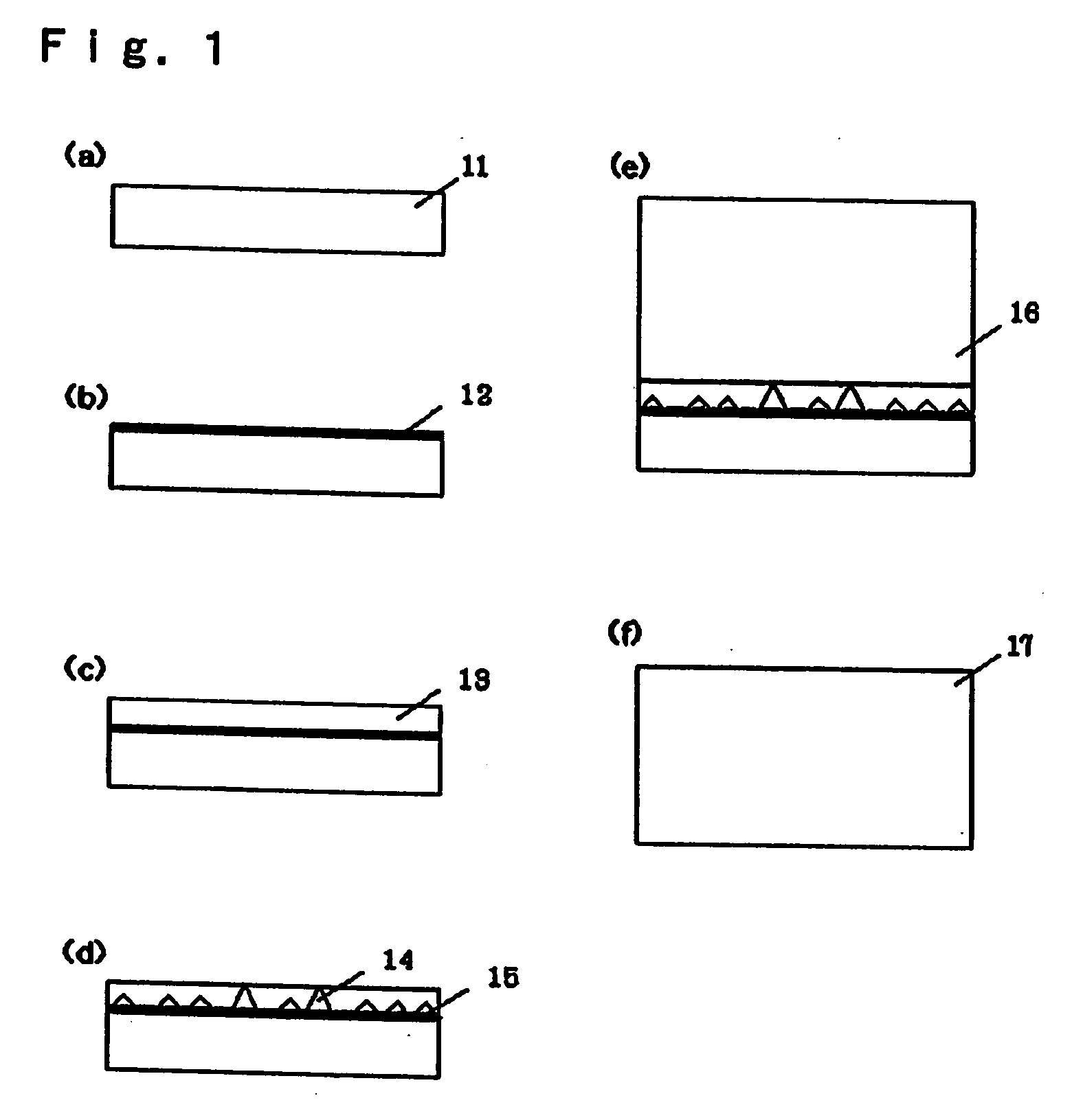
embodiment 1
[0135] The present embodiment 1 belongs to type I mentioned above. First, Ti is deposited on a sapphire substrate by evaporation. Then, a GaN film is grown thereon at a low temperature. Thereafter, it is heated up to generate voids in the low temperature grown GaN. Successively, a thick film of GaN is grown over at a high temperature; and after that, the sapphire substrate is removed by spontaneous peeling or etching to obtain a self-supported substrate.
embodiment 2
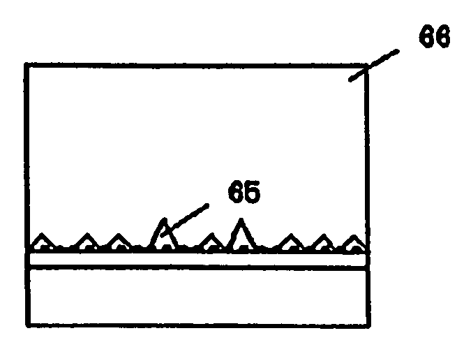
[0136] The present embodiment 2 belongs to the aborementioned type II. The embodiment 2 is a process in which voids are formed above the metal element-containing film without any nitrification treatment. The present inventors have found that a thin film of metal material or of metal nitride being not lattice-matched with the surface of base substrate (in case that the metal element-containing film is formed directly on a hetero-substrate, with the surface of hetero-substrate, or else in case that a group III nitride semiconductor film has been formed on a hetero-substrate, with the group III nitride semiconductor film) is formed, and thereby the thin film having a fine pore structure can be prepared. In this case, there is no necessity that after the thin film of metal or metal nitride is formed, the film is always subjected to a nitrification treatment or a heat treatment. As the thin film of metal or metal nitride is different from the base substrate in crystal structure and latti...
embodiment 3
[0138] The embodiment 3 belongs to type III explained above. The pre-step of heating up for growth of a layer of the nitride may be conducted using only a H2 atmosphere. By selecting this condition, before being buried, the surface of TiN is exposed to a H2 atmosphere to promote the elimination of N, whereby Ti can be partially exposed thereon. As a result, the decomposing action for group III nitride semiconductor, which Ti possesses, becomes striking, and thereby region of voids are formed preferably.
[0139] In the present embodiment, when a layer of the nitride semiconductor is grown on the metal element-containing film, the V / III ratio is set at <10 at least at the initial stage of the growth. By conducting the growth under a condition relatively rich in Ga, elimination of N from TiN is promoted at the initial stage of growth, whereby Ti of high catalytic activity can be exposed at the surface thereof.
PUM
| Property | Measurement | Unit |
|---|---|---|
| temperature | aaaaa | aaaaa |
| temperature | aaaaa | aaaaa |
| thickness | aaaaa | aaaaa |
Abstract
Description
Claims
Application Information