Supercharge Your Innovation With Domain-Expert AI Agents!

Non-volatile storage device

Active Publication Date: 2012-06-28
LAPIS SEMICON CO LTD
View PDF1 Cites 1 Cited by
  • Summary
  • Abstract
  • Description
  • Claims
  • Application Information

AI Technical Summary

Benefits of technology

[0015]According to the present invention an effect is exhibited in which access delay can be suppressed from occurring.

Problems solved by technology

This is one cause of access delay.
However, the magnitude of the internal voltage CSV does not always match the magnitude of a reference voltage.
An issue thus arises with such a related non-volatile memory in that sometimes an access delay arises due to the magnitude of the internal voltage CSV and the magnitude of the reference voltage not always matching.

Method used


Image

  • Non-volatile storage device
  • Non-volatile storage device
  • Non-volatile storage device

Examples


first exemplary embodiment

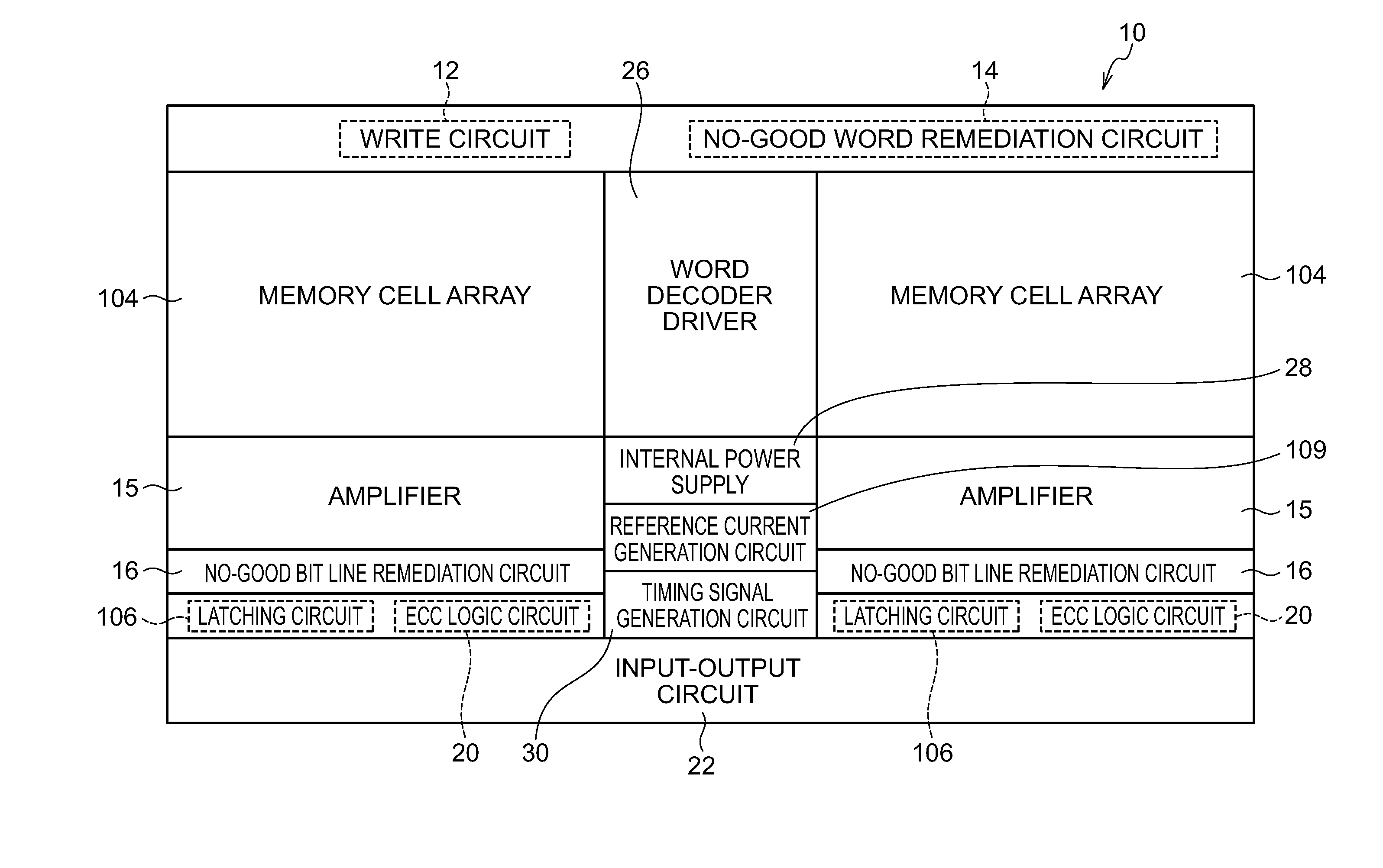
[0036]FIG. 1 schematically illustrates an example of a configuration of a non-volatile memory 10 according to a first exemplary embodiment of the present invention. As shown in FIG. 1, the non-volatile memory 10 is equipped with plural memory cell arrays 104. The plural memory cell arrays 104 are provided with a common write circuit 12 and a common fail word redundancy circuit 14. The write circuit 12 is a circuit for applying a voltage to the memory cells 102 in order to re-write data. The fail word redundancy circuit 14 is a redundancy circuit for performing remediation by employing a reserve word line when a fail word line WL arises.

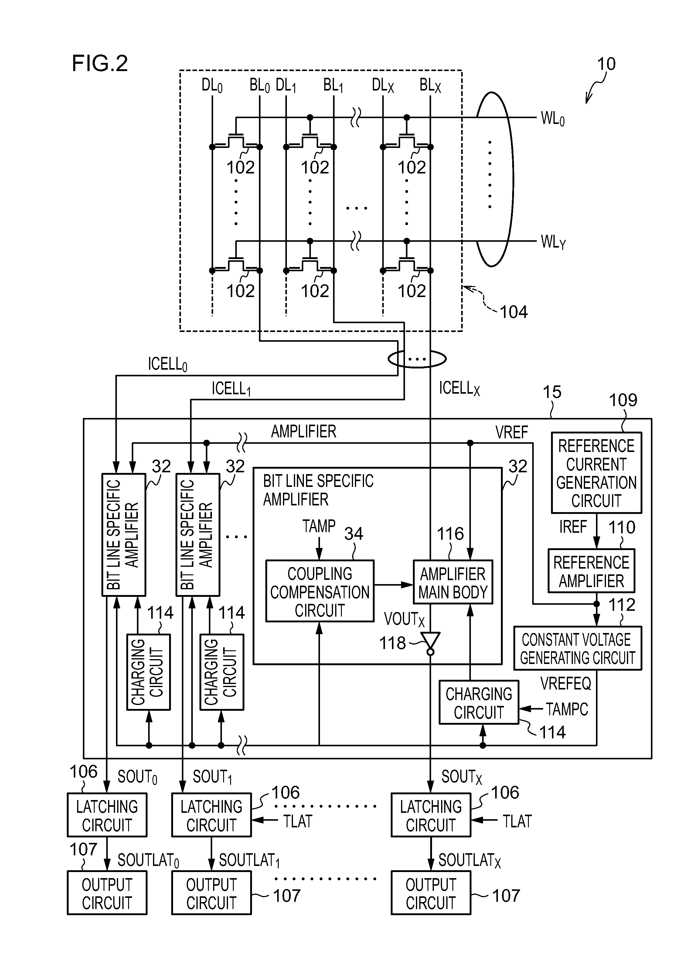
[0037]Each of the memory cell arrays 104 is provided with an amplifier 15, a fail bit line redundancy circuit 16, a latching circuit 106 and an ECC logic circuit 20. Each of the amplifiers 15 is equipped with the functions of the amplifier 105 illustrated in FIG. 8. Each of the fail bit line redundancy circuits 16 is a redundancy circuit for performin...

second exemplary embodiment

[0079]The non-volatile memory according to a second exemplary embodiment differs from the non-volatile memory 10 according to the first exemplary embodiment in that an amplifier 80 is applied in place of the amplifier 15. The same reference numerals are accordingly applied to similar configuration elements to those of the non-volatile memory 10 of the first exemplary embodiment, and further explanation thereof is omitted. Explanation follows regarding points that differ from the non-volatile memory 10 according to the first exemplary embodiment.

[0080]FIG. 5 is a diagram illustrating an example of a configuration of the amplifier 80 according to the second exemplary embodiment. As shown in FIG. 5, the amplifier 80 differs from the amplifier 15 illustrated in FIG. 3 in that a bit line specific amplifier 82 is applied in place of the bit line specific amplifier 32. The bit line specific amplifier 82 differs from the bit line specific amplifier 32 illustrated in FIG. 3 in that instead o...


PUM


Abstract

There is provided a non-volatile storage device including: a bit line that is connected to a non-volatile storage element and is applied with a voltage of magnitude corresponding to the logic value stored in the storage element; a charging section that charges the bit line to a voltage of equivalent magnitude to the reference voltage; a voltage generation section that is connected between the reference voltage line and the bit line, comprises a capacitance load for generating coupling charge when charging by the charging section has been performed, and employs the capacitance load to generate a voltage according to a difference between the magnitude of the voltage of the reference voltage line and the magnitude of the voltage of the bit line as a voltage expressing the comparison result; and a charge absorbing section for absorbing the coupling charge generated by the capacitance load.

Description

CROSS-REFERENCE TO RELATED APPLICATION[0001]This application is based on and claims priority under 35 USC 119 from Japanese Patent Application No. 2010-285916 filed on Dec. 22, 2010, the disclosure of which is incorporated by reference herein.BACKGROUND[0002]1. Technical Field[0003]The present invention relates to an electrically writable non-volatile storage device.[0004]2. Related Art[0005]A known related non-volatile memory is one in which, for example, plural memory cells are disposed at word lines WL and bit lines BL so as to form a memory array. Data is read out therefrom by sequentially connecting a read-out amplifier through a selection circuit to the bit line BL of the memory cell to be read out, and using the read-out amplifier to compare the magnitude of the voltage of the bit line connected to the memory cell against the magnitude of a reference voltage.[0006]The memory cells are stored with data representing logic values of “1” or “0”. The magnitude of the voltage of th...

Claims


Application Information

Patent Timeline
IPC IPC(8): G11C16/06
CPCG11C16/24G11C7/062G11C16/28
Inventor TANIKAWA, HIROYUKIKURAMORI, BUNSHO
Owner LAPIS SEMICON CO LTD
Features
  • R&D
  • Intellectual Property
  • Life Sciences
  • Materials
  • Tech Scout
  • Unparalleled Data Quality
  • Higher Quality Content
  • 60% Fewer Hallucinations
Learn More