
Charge pump circuit

a charge pump and circuit technology, applied in the direction of electric variable regulation, process and machine control, instruments, etc., can solve the problems of increasing the demands of users for reducing audio artefacts, increasing physical size and cost, and audible pops, clicks and other audio artefacts

Active Publication Date: 2012-06-28
CIRRUS LOGIC INC
View PDF4 Cites 13 Cited by
  • Summary
  • Abstract
  • Description
  • Claims
  • Application Information

AI Technical Summary

Benefits of technology

[0022]According to an aspect of the present invention, there is provided a charge pump circuit, comprising: an input node and a reference node for connection to an input voltage; a first pair of output nodes and a second pair of output nodes; two pairs of flying capacitor nodes; a network of switching paths for interconnecting

Problems solved by technology

It is well known in the art that this series connected coupling capacitor needs to be a large value to allow adequate bass response, and so tends to be physically large and expensive.
Also on power-up and power down charging this capacitor up to its quiescent voltage of VV / 2 is liable to cause audible pops, clicks and other audio artefacts in the audio output signal 15.
Techniques are known to reduce these artefacts, but in practice cannot remove them completely, and demands of users for reduced audio artefacts are becoming ever more stringent.
This analogue level shift is undesirable, as any shift from VV / 2 to ground may lead to some voltage drop across some resistance, and hence power will be wasted.
Even if the supply voltage (VP, VN) can be halved using the aforesaid known charge pump described above, then the efficiency is still poor, and reducing the power supply further makes it difficult practically to get enough voltage headroom for the input stage of amplifier 24.
Further, especially at low signal levels, the power required to switch the switching devices of the charge pump may be significant enough to degrade the efficiency.
These flying capacitors are generally too large to be accommodated on-chip, so require dedicated pins on the package a well as occupying area on the PCB.

Method used


Image

  • Charge pump circuit
  • Charge pump circuit
  • Charge pump circuit

Examples


Embodiment Construction

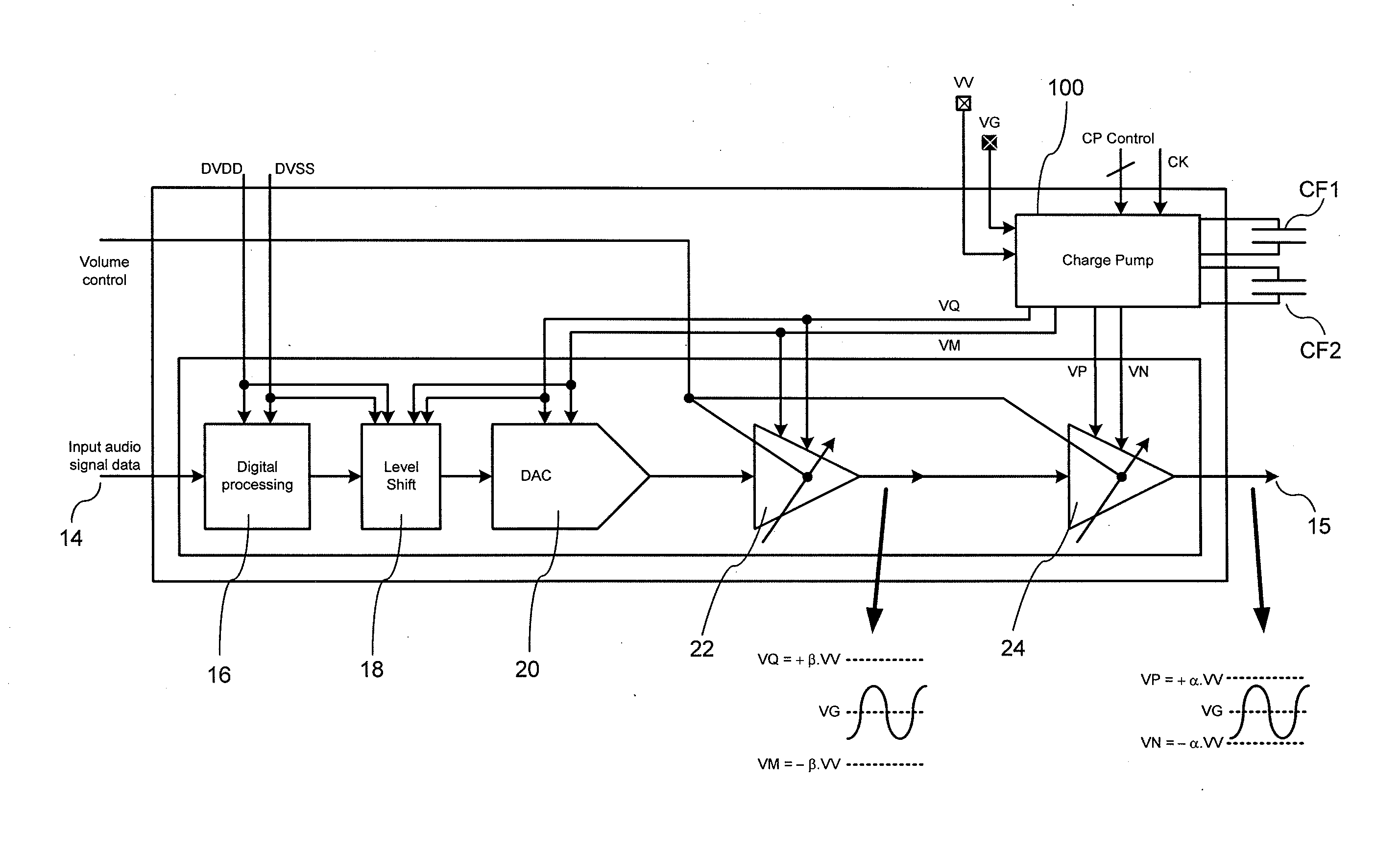
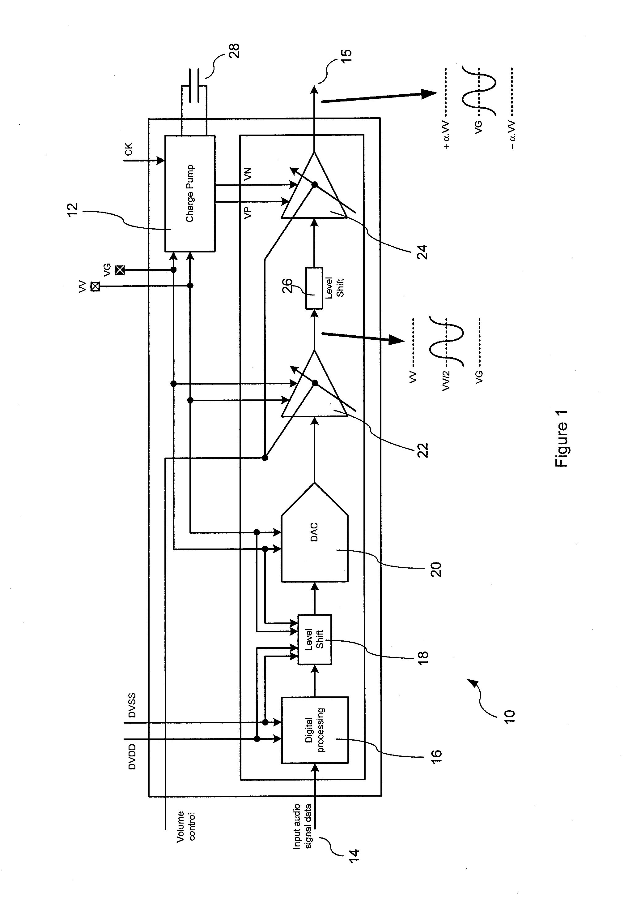
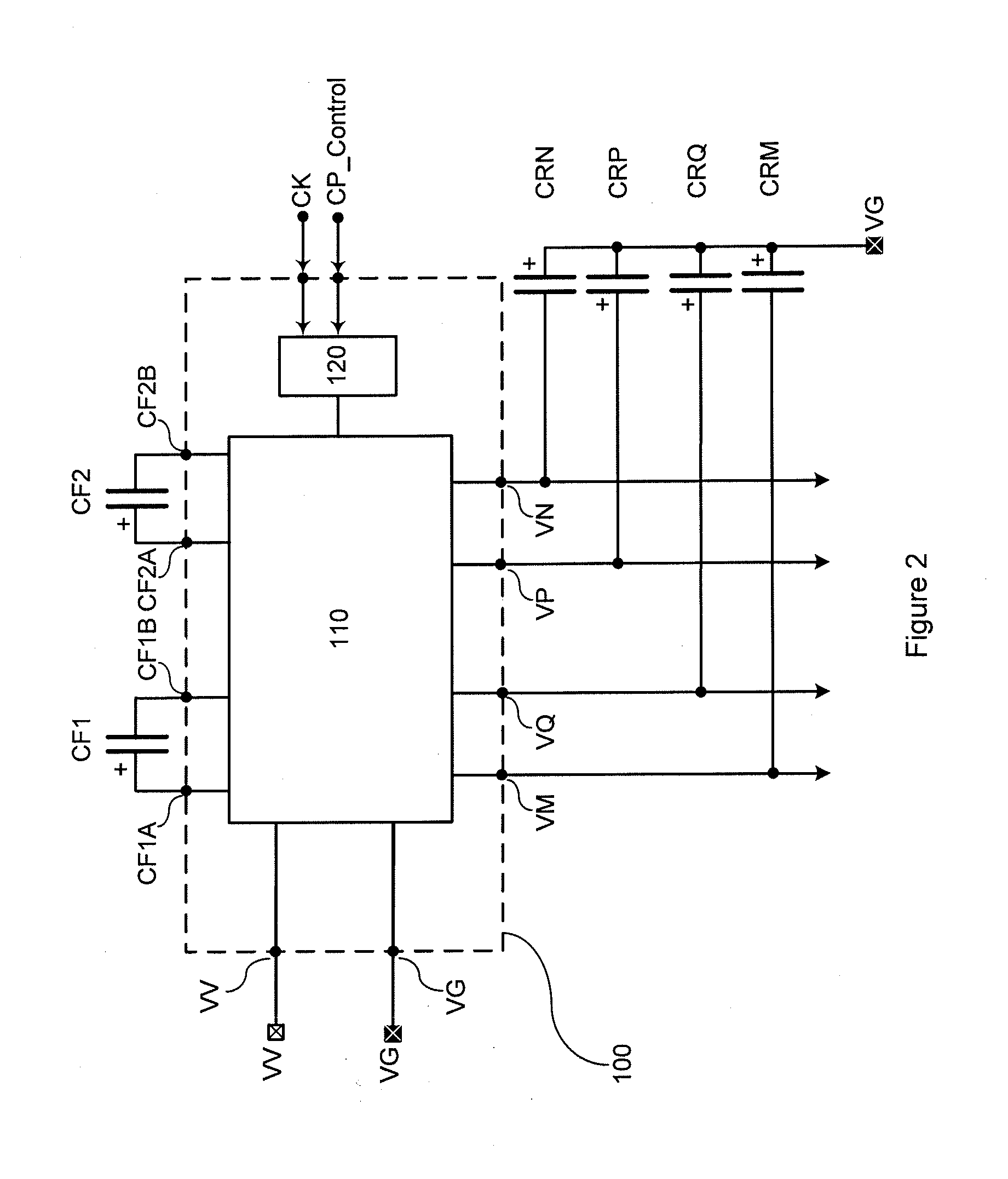
[0124]FIG. 2 schematically shows a charge pump circuit 100 that includes a plurality of nodes and a network of switching paths, i.e. a switch matrix or network of switches or switching network, 110, for selective connection of the plurality of nodes and a controller 120 for controlling the network of switching paths. The charge pump circuit 100 includes an input node (VV) for receiving an input voltage, a reference node (VG) for receiving a reference voltage, a first flying capacitor node (CF2A) and a second flying capacitor node (CF2B) for connection with a first flying capacitor (CF2), a third flying capacitor node (CF1A) and a fourth flying capacitor node (CF1B) for connection with a second flying capacitor (CF1), a first pair of output nodes comprising a first output node (VP) and a second output node (VN), and a second pair of output nodes comprising a third output node (VQ) and a fourth output node (VM).

[0125]As shown in FIG. 2 and throughout the figures, the input node VV is ...


PUM


Abstract

A bipolar output charge pump circuit 100 having a network of switching paths 110 for selectively connecting an input node (VV) and a reference node (VG) for connection to an input voltage, a first pair of output nodes (VP, VN) and a second pair of output nodes (VQ, VM), and two pairs of flying capacitor nodes (CF1A, CF1 B; CF2A, CF2B), and a controller for controlling the switching of the network of switching paths. The controller is operable to control the network of switching paths when in use with two flying capacitors (CF1, CF2) connected to the two pairs of flying capacitor nodes, to provide a first bipolar output voltage at the first pair of output nodes (VP, VN) and a second bipolar output voltage at the second pair of bipolar output nodes (VQ, VM).

Description

[0001]This is a continuation of U.S. application Ser. No. 13 / 336,795, filed Dec. 23, 2011, now abandoned, which claims the benefit of U.S. Provisional Application No. 61 / 427,431, filed on Dec. 27, 2010.BACKGROUND OF THE INVENTION[0002]1. Field of the Invention[0003]Aspects of the present invention relate to a bipolar output voltage charge pump circuit and more particularly, they relate to a bipolar output voltage charge pump circuit which provides two bipolar output voltages, i.e. two pairs of opposite polarity output voltages.[0004]2. Description of the Related Art[0005]Bipolar, i.e. dual rail, output voltage charge pump circuits are a type of DC-DC converter that utilize transfer and storage capacitors as devices to respectively transfer and store energy such that the converter is able to provide, from a unipolar, i.e. single rail, input voltage source, a bipolar output voltage that may be different in value from that of the unipolar input voltage.[0006]In use, single bipolar outp...

Claims


Application Information

Patent Timeline
IPC IPC(8): H03G3/00G05F1/10H02M1/00
CPCH02M3/07H02M2001/0083H03F3/181H02M2001/009H02M1/009H02M1/0083H02M3/071H02M3/072H02M1/00
Inventor LESSO, JOHN PAULFRITH, PETER JOHNPENNOCK, JOHN LAURENCE
Owner CIRRUS LOGIC INC
Learn More