Unlock instant, AI-driven research and patent intelligence for your innovation.

Field effect transistor having ohmic body contact(s), an integrated circuit structure incorporating stacked field effect transistors with such ohmic body contacts and associated methods

Active Publication Date: 2012-07-05
GLOBALFOUNDRIES US INC
View PDF0 Cites 9 Cited by
  • Summary
  • Abstract
  • Description
  • Claims
  • Application Information

AI Technical Summary

Benefits of technology

[0007]In view of the foregoing disclosed herein are embodiments of a field effect transistor (FET) structure, in which ohmic body contact(s) are placed relatively close to (e.g., within 1.00 μm of) the active region of the FET. The FET can comprise a semiconductor layer, in which an active region and body contact region(s) are defined by a trench isolation structure and in which a body region is below and abuts the active region, the trench isolation structure and the body contact region(s). A gate structure can traverse the active region. Additionally, dummy gate structure(s) can be positioned on the body contact region(s). A contact can extend through each dummy ga

Problems solved by technology

Furthermore, such threshold voltage variations can differ between PDSOIFETs at different locations within an electronic circuit and can, thereby degrade the performance of the electronic circuit.
Unfortunately, this solution adds to the area of the wafer consumed by the FET.
However, this solution involves additional processing steps that add to processing time and costs.

Method used


Image

  • Field effect transistor having ohmic body contact(s), an integrated circuit structure incorporating stacked field effect transistors with such ohmic body contacts and associated methods
  • Field effect transistor having ohmic body contact(s), an integrated circuit structure incorporating stacked field effect transistors with such ohmic body contacts and associated methods
  • Field effect transistor having ohmic body contact(s), an integrated circuit structure incorporating stacked field effect transistors with such ohmic body contacts and associated methods

Examples


Embodiment Construction

[0046]The embodiments of the invention and the various features and advantageous details thereof are explained more fully with reference to the non-limiting embodiments that are illustrated in the accompanying drawings and detailed in the following description.

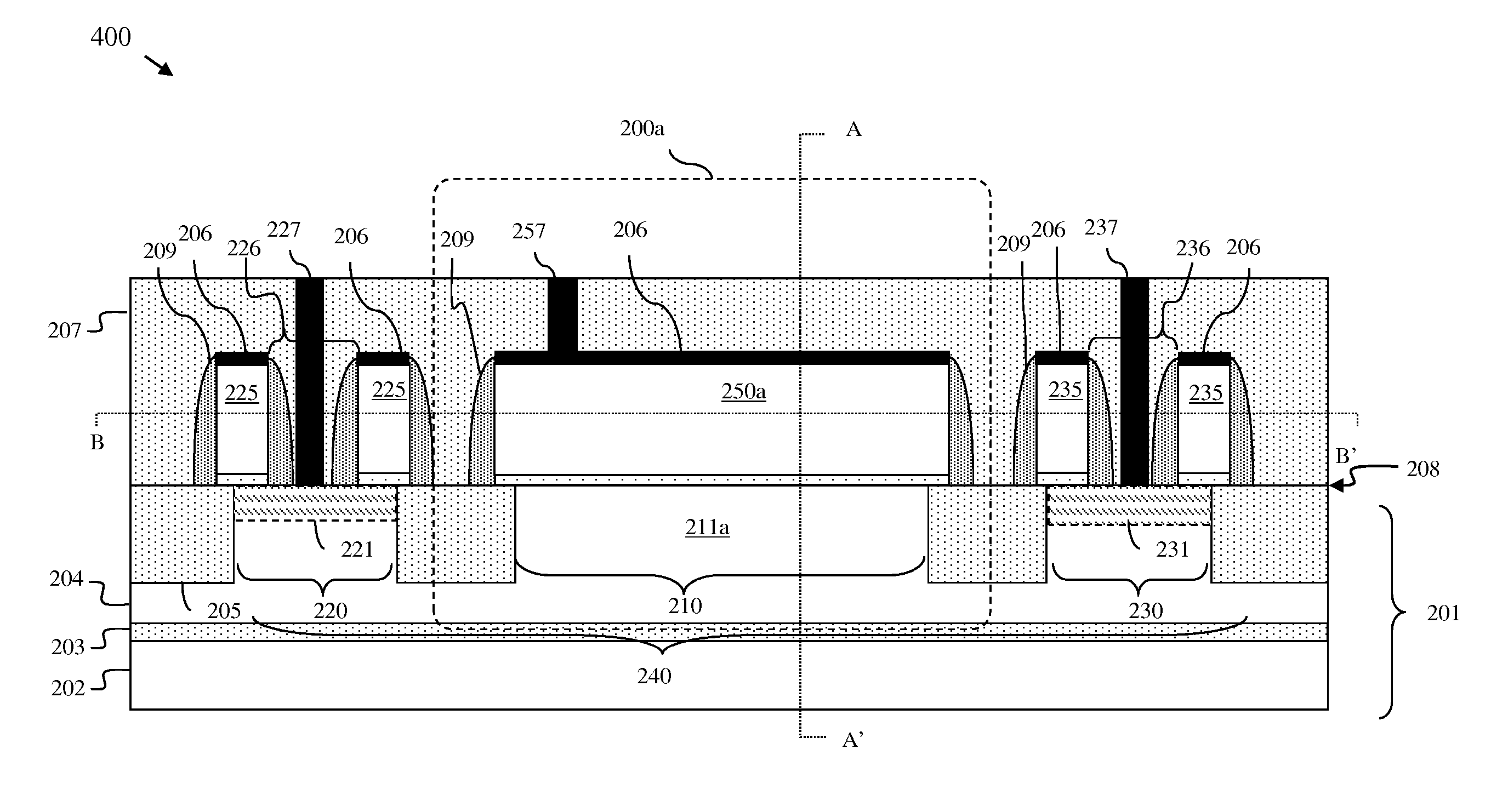
[0047]As mentioned above, the body contacts for partially-depleted semiconductor-on-insulator field effect transistors (PDSOIFETs) must be ohmic contacts so that the current-voltage (I-V) curve is linear and symmetric and also to avoid snapback. To achieve an ohmic body contact, it is necessary to avoid placing the contact on an area of the device implanted with source / drain or source / drain extension dopants. This is because an area of the device implanted with such dopants will have an opposite conductivity type than the body of the FET, thereby forming a PN junction which blocks the connection between the contact and the body. In FETs designed for high-voltage applications, a heavily tilted implant process is used to form de...


PUM


Abstract

Disclosed is a field effect transistor (FET), in which ohmic body contact(s) are placed relatively close to the active region. The FET includes a semiconductor layer, where the active region and body contact region(s) are defined by a trench isolation structure and where a body region is below and abuts the active region, the trench isolation structure and the body contact region(s). A gate traverses the active region. Dummy gate(s) are on the body contact region(s). A contact extends through each dummy gate to the body contact region below. Dielectric material isolates the contact(s) from the dummy gate(s). During processing, the dummy gate(s) act as blocks to ensure that the body contact regions are not implanted with source / drain dopants or source / drain extension dopants and, thereby to ensure that the body contacts, as formed, are ohmic. Also disclosed are an integrated circuit structure with stacked FETs, having such ohmic body contacts, and associated methods.

Description

BACKGROUND[0001]1. Field of the Invention[0002]The present invention relates to field effect transistors and, more particularly, to embodiments of a field effect transistor (FET) structure having one or more ohmic body contacts placed relatively close to the active region of the FET, to embodiments of an integrated circuit structure incorporating a plurality of stacked FETs with such ohmic body contacts and to method embodiments for forming these structures.[0003]2. Description of the Related Art[0004]A semiconductor-on-insulator (SOI) field effect transistor (FET) is a FET formed in the semiconductor layer of a semiconductor-on-insulator wafer. Shallow trench isolations (STI) structures extend through the semiconductor layer and isolated the SOI FET from other devices within the semiconductor layer. As with any FET, an SOIFET comprises a channel region positioned between source / drain regions and a gate structure positioned above the channel region. However, depending upon the confi...

Claims


Application Information

Patent Timeline
IPC IPC(8): H01L27/088H01L21/336H01L21/8234H01L29/78
CPCH01L21/743H01L29/7833H01L21/823481H01L21/823475
Inventor ABOU-KHALIL, MICHEL J.CLARK, JR., WILLIAM F.SHI, YUN
Owner GLOBALFOUNDRIES US INC
Features
  • R&D
  • Intellectual Property
  • Life Sciences
  • Materials
  • Tech Scout
  • Unparalleled Data Quality
  • Higher Quality Content
  • 60% Fewer Hallucinations
Learn More