Flip chip device having simplified routing

a chip device and chip chip technology, applied in semiconductor devices, semiconductor/solid-state device details, electrical devices, etc., can solve the problem and achieve the effect of shortening the routing line length

Active Publication Date: 2012-07-05
STMICROELECTRONICS INT NV
View PDF4 Cites 5 Cited by
  • Summary
  • Abstract
  • Description
  • Claims
  • Application Information

AI Technical Summary

Benefits of technology

[0010]Providing the bump pads on each side of the input / output contact pads increases the number of bump pads in close proximity to the input / output contact pads, which results in shorter routing line length. This also decreases a density of the second plurality of bump pads, which are positioned interior to the input / output contact pads. This reduced density allows for wider routing lines into the interior of the die.

Problems solved by technology

Providing the bump pads on each side of the input / output contact pads increases the number of bump pads in close proximity to the input / output contact pads, which results in shorter routing line length.

Method used


Image

  • Flip chip device having simplified routing
  • Flip chip device having simplified routing
  • Flip chip device having simplified routing

Examples


Embodiment Construction

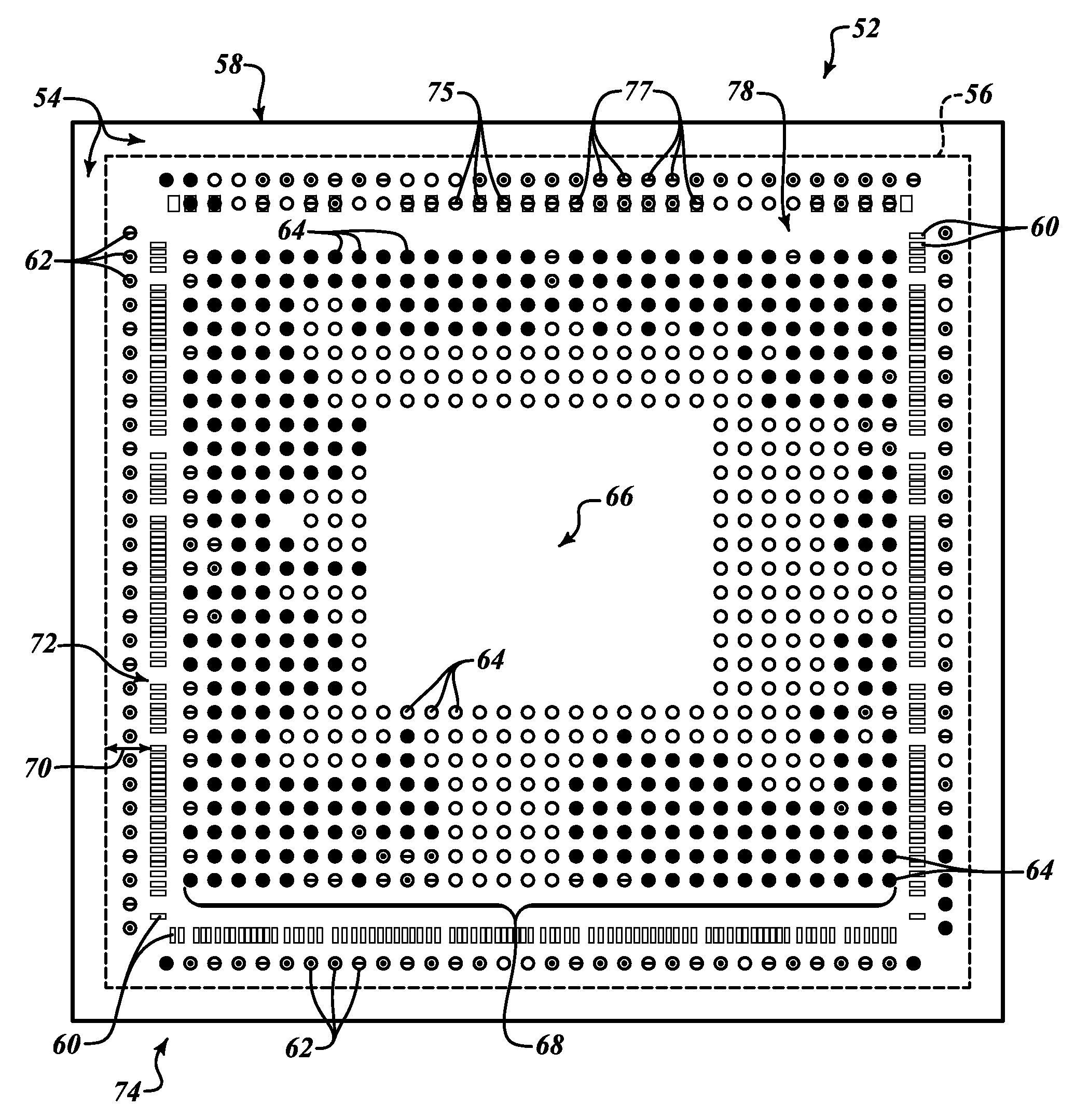
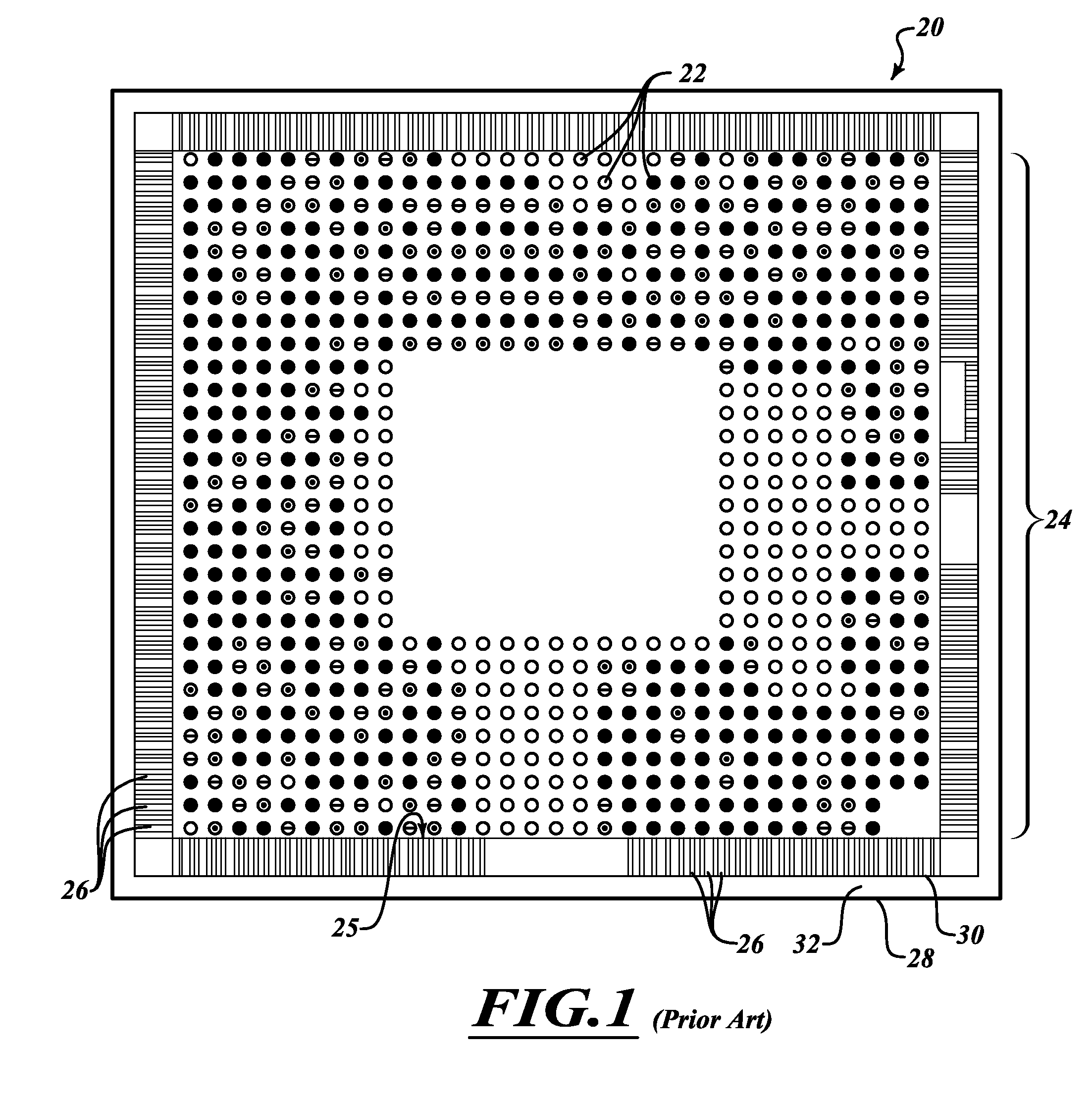
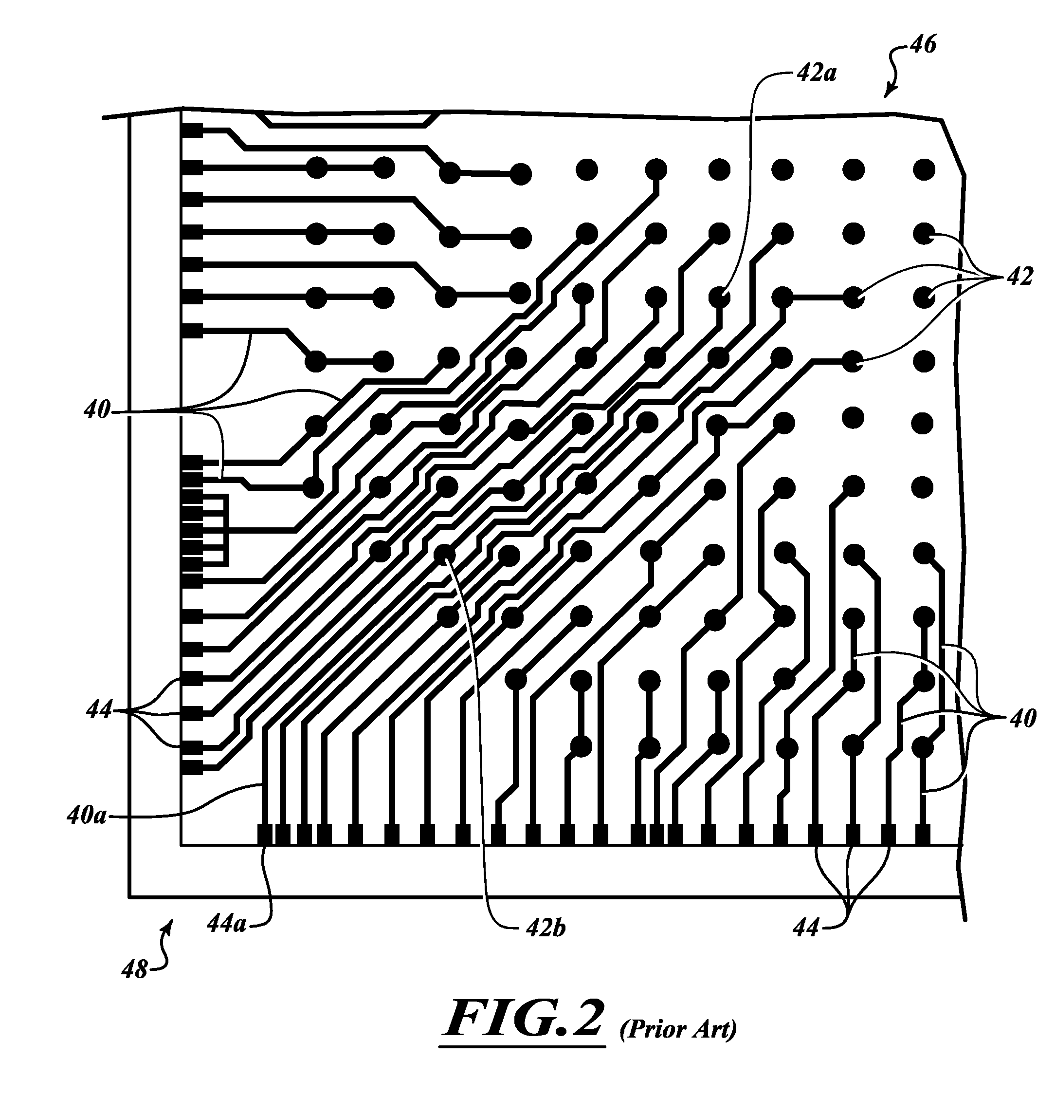
[0022]In the following description, certain specific details are set forth in order to provide a thorough understanding of various embodiments of the disclosure. However, one skilled in the art will understand that the disclosure may be practiced without these specific details. In some instances, well-known structures associated with the manufacturing of semiconductor wafers have not been described in detail to avoid obscuring the descriptions of the embodiments of the present disclosure.

[0023]Unless the context requires otherwise, throughout the specification and claims that follow, the word “comprise” and variations thereof, such as “comprises” and “comprising,” are to be construed in an open, inclusive sense, that is, as “including, but not limited to.”

[0024]Reference throughout this specification to “one embodiment” or “an embodiment” means that a particular feature, structure, or characteristic described in connection with the embodiment is included in at least one embodiment. ...


PUM


Abstract

The present disclosure is directed to a semiconductor die having a chip outline boundary, a die seal, a row of input/output contact pads separated from the chip outline boundary by the die seal, a first row of solder bump connections positioned between the row of input/output contact pads and the die seal, and a second row of solder bump connections separated from the first row of solder bump connections by the row of input/output contact pads.

Description

BACKGROUND[0001]1. Technical Field[0002]The present disclosure is directed to a flip chip device having simplified routing demands, and more particularly, to a die having a first plurality of bump pads between a die seal and a plurality of input / output contact pads.[0003]2. Description of the Related Art[0004]FIG. 1 is a first die 20 having a plurality of solder bumps 22 formed in an array 24 within an internal edge 25 of a plurality of contact pads 26 in a known flip-chip design. Flip chip is a method of electrically connecting the first die 20 to a package carrier, which is either a substrate or a lead frame. This method addresses problems that arise from higher integration density and rising power consumption. Flip chip is particularly beneficial for high speed applications and has the following advantages: reduced signal inductance, reduced power and ground inductance, reduced package footprint, smaller die size, shorter wire lengths, higher signal density, and lower thermal eff...

Claims


Application Information

Patent Timeline
Patent Type & Authority Applications(United States)
IPC IPC(8): H01L23/485H01L21/441
CPCH01L23/525H01L24/13H01L2924/00014H01L2924/01029H01L2224/06157H01L2924/014H01L2224/05569H01L2224/02379H01L23/585H01L24/05H01L24/06H01L2224/02381H01L2224/0239H01L2224/0401H01L2224/06155H01L2224/131H01L2224/05572H01L2224/05552H01L2924/14H01L2924/00
Inventor YADAV, ANILJAIN, SANJEEV KUMARBAJAJ, RAJESH
Owner STMICROELECTRONICS INT NV
Why Eureka
Try Eureka