Organic el display panel and method for producing same

a technology of organic el and display panels, which is applied in the direction of thermoelectric device junction materials, electrical apparatus, and semiconductor devices, etc., can solve the problems of preventing the improvement of luminous efficiency and hindering the improvement of aperture ratio, so as to improve the aperture ratio, improve the luminous efficiency, and the aperture is larger.

Active Publication Date: 2012-07-12
JOLED INC
View PDF2 Cites 11 Cited by
  • Summary
  • Abstract
  • Description
  • Claims
  • Application Information

AI Technical Summary

Benefits of technology

[0008]According to the above aspect of the present invention, in the organic EL display panel having the above structure, each aperture defined by the bank per pixel includes a contact hole. This structure allows the apertures to be larger and the aperture ratio to improve as compared with conventional structures. Consequently, the light-emitting surface area increases and thus the luminous efficiency improves. More specifically, in each aperture, the organic light-emitting layer is thicker at a portion located within the contact hole region than at a portion located outside the contact hole region. This prevents concentration of the electric field along the slanted surface that extends from the upper periphery of the contact hole to the bottom surface of the contact hole, in particular around the upper periphery of the contact hole.
[0009]Furthermore, since the organic light-emitting layer formed in each aperture has a thicker portion in the contact hole region than the other portion located outside the contact hole region, the electric field in each contact hole region is smaller as compared to the region other than the contact hole region. Accordingly, while the organic light-emitting layer emits light in the region other than the contact hole region, the organic light-emitting layer either does not emit light in the contact hole region or emits light at a lower luminance than in the region other than the contact hole region. However, the contact hole region occupies only a very small area within the aperture, and therefore even if the contact hole region does not emit light, or emits light at a low luminance, there is little overall effect on the aperture as a whole. That is, the presence of the contact hole regions does not cause reduction of the overall luminescence brightness. Therefore, by locating the contact holes beneath the apertures defined one for each pixel by the bank, the aperture ratio increases and thus the luminescence brightness improves.

Problems solved by technology

However, such a structure hinders improvement of aperture ratio, which prevents an increase in the light-emitting surface area in an organic EL display panel and prevents improvement of luminous efficiency (see Patent Literature 1).

Method used


Image

  • Organic el display panel and method for producing same
  • Organic el display panel and method for producing same
  • Organic el display panel and method for producing same

Examples


embodiment 1

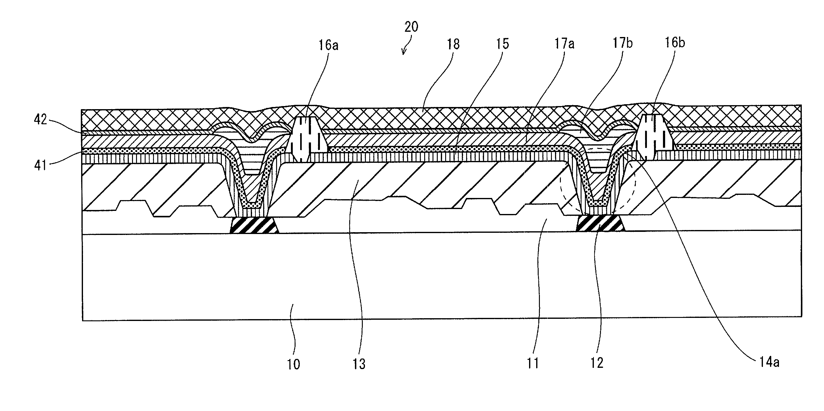
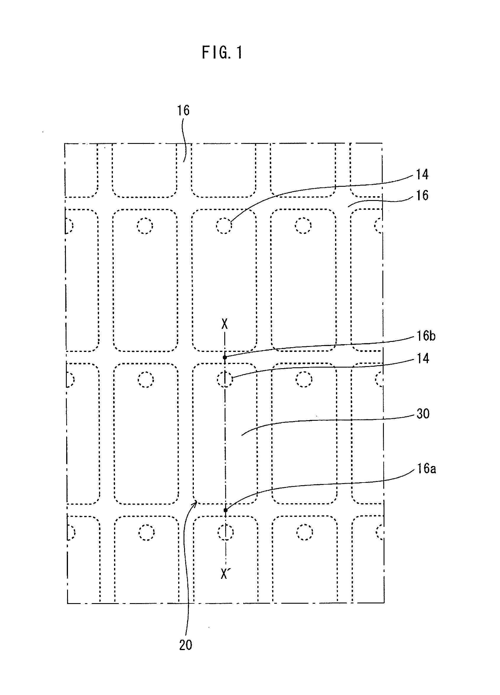
[0089]FIG. 5C is a schematic top view showing an aperture 30 and the surrounding area when a contact hole is simply provided within the aperture without adopting the structure in

[0090]Each diagonally shaded area shown in FIG. 5C corresponds to the inner region 14f near the contact hole upper periphery 14a shown in FIGS. 3A and 3B. As described above, the light-emitting layer 17a is thinner in the area than the ordinal thickness, and therefore due to concentration of the electric field, the luminescence brightness increases more than usual. An increase in luminescence brightness is visible even in a minute area, and therefore irregular light emission in this section ends up being conspicuous.

[0091]FIGS. 6A to 6E and 7A to 7C are views illustrating processing steps of a method of manufacturing the organic EL display panel according to an embodiment of the present invention.

[0092]The method includes the first to seventh steps.

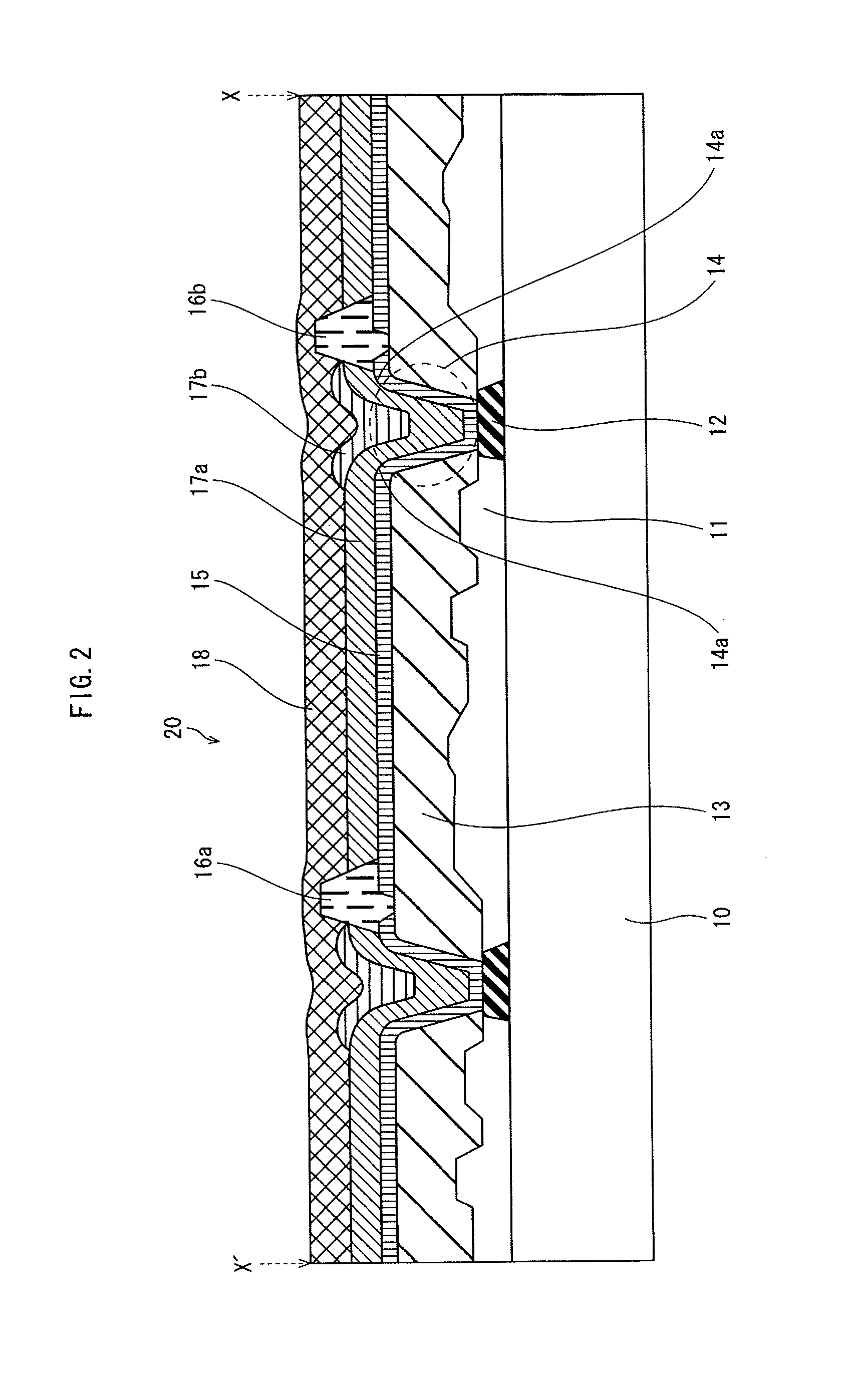
[0093]First, in the first step shown in FIG. 6A, the TFT lay...


PUM


Abstract

Provided is an organic EL display panel that improves aperture ratio by providing a contact hole beneath an aperture in a bank, and that prevents shortening of the display panel's lifetime by avoiding electric field concentration. An organic EL display panel includes a TFT layer; an interlayer insulation film on the TFT layer and having a plurality of contact holes one per pixel; a plurality of first electrodes, one per pixel, on the interlayer insulation film; a bank defining a plurality of apertures, at least one per pixel, and at least one contact hole is located beneath each aperture; a plurality of organic light-emitting layers each in an aperture; and a second electrode above the organic light-emitting layers. In each aperture, a thickness of the organic light-emitting layer is greater at a portion within the contact hole region than at a portion outside the contact hole region.

Description

CROSS REFERENCE TO RELATED APPLICATION[0001]This is a continuation application of PCT Application No. PCT / JP2010 / 003123 filed May 7, 2010, designating the United States of America, the disclosure of which, including the specification, drawings and claims, is incorporated herein by reference in its entirety.TECHNICAL FIELD[0002]The present invention relates to an organic EL display panel and in particular to technology for improving aperture ratio.BACKGROUND ART[0003]In recent years, research and development has progressed in the area of organic electroluminescence (hereinafter “organic EL”) display panels that use the phenomenon of electroluminescence of organic material. Each organic EL cell of an organic EL display panel has an anode, a cathode, and an organic light-emitting layer provided between the anode and the cathode. The anode is layered on an interlayer insulation film that is layered on a Thin Film Transistor (TFT) substrate for driving the cells. To connect the anode wit...

Claims


Application Information

Patent Timeline
Patent Type & Authority Applications(United States)
IPC IPC(8): H01L27/32H01L51/56
CPCH01L27/3246H01L27/3258H01L27/3248H10K59/123H10K59/124H10K59/122
Inventor TAKEUCHI, TAKAYUKI
Owner JOLED INC
Why Eureka
Try Eureka