Semiconductor device, semiconductor package, and method for manufacturing semiconductor device

Inactive Publication Date: 2012-07-12
PANASONIC CORP
View PDF4 Cites 0 Cited by
  • Summary
  • Abstract
  • Description
  • Claims
  • Application Information

AI Technical Summary

Benefits of technology

[0017]In the semiconductor device of the present invention, all of the two main surfaces and the side surfaces of the semiconductor element other than the first main surface covered with the encapsulation resin can be exposed, whereby the heat dissipation capability of the mounted semiconductor element can be improved. Also, the semiconductor element and the circuit board are arranged side by side, whereby the flexibility of interconnect design of the semiconductor element and the circuit board and the productivity of the semiconductor element during a mounting step both can be improved.
[0018]Also, in the semi

Problems solved by technology

In recent years, as the functions of electronic apparatuses have advanced quickly, the po

Method used


Image

  • Semiconductor device, semiconductor package, and method for manufacturing semiconductor device
  • Semiconductor device, semiconductor package, and method for manufacturing semiconductor device
  • Semiconductor device, semiconductor package, and method for manufacturing semiconductor device

Examples


Example

First Embodiment

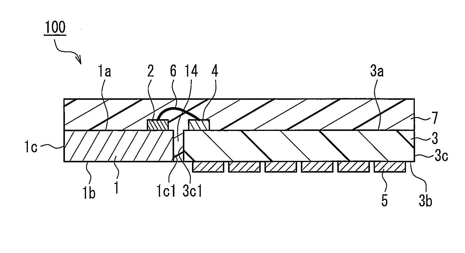
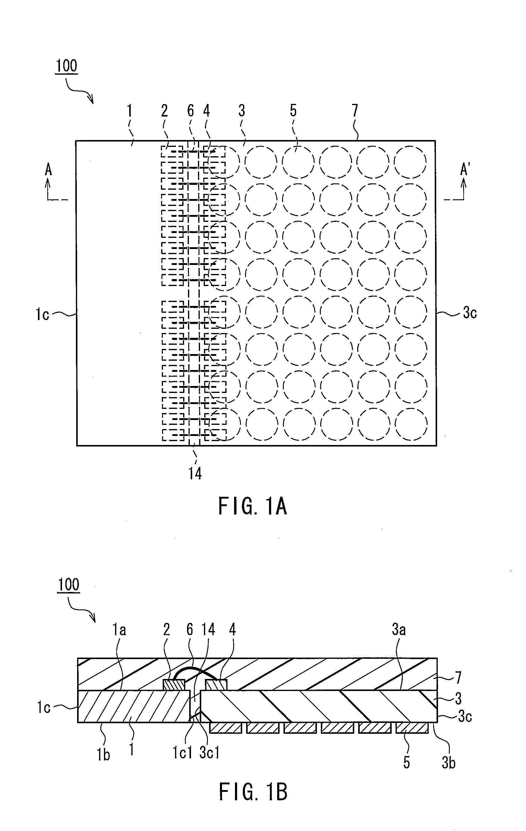
[0056]Firstly, as a first embodiment of the present invention, a configuration of the semiconductor device of the present invention will be described.

[0057]FIG. 1 is a diagram showing a configuration of a semiconductor device 100 according to the first embodiment. FIG. 1A is a plan view of the configuration as viewed from above a first main surface of the semiconductor device 100. FIG. 1B is a cross-sectional view of the configuration taken along arrowed line A-A′ of FIG. 1A.

[0058]As shown in FIG. 1, the semiconductor device 100 of this embodiment includes: a semiconductor element 1 having a first main surface 1a on which connection electrodes 2 are formed, a second main surface 1b opposite to the first main surface 1a, and side surfaces 1c substantially perpendicular to the first main surface 1a and the second main surface 1b; and a circuit board 3 having a first main surface 3a on which electrode pads 4 are formed, a second main surface 3b opposite to the first mai...

Example

Second Embodiment

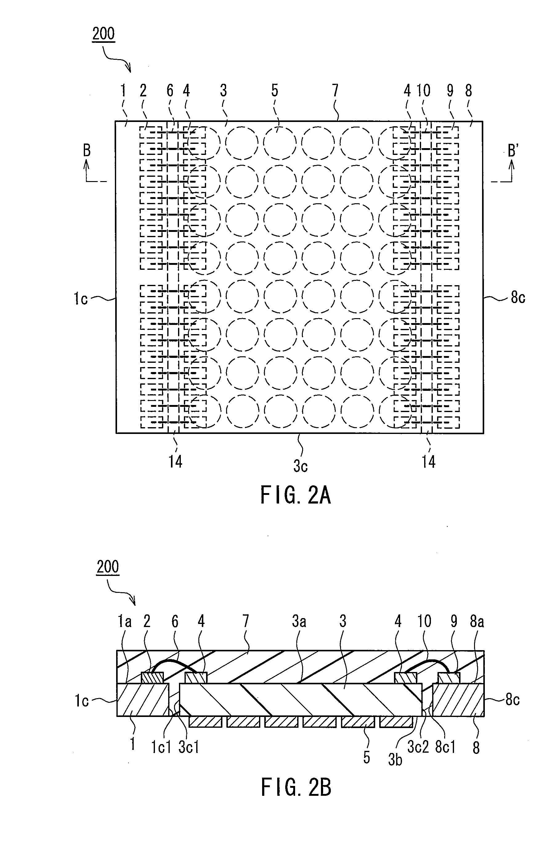
[0099]Next, as a second embodiment of the present invention, another example configuration of the semiconductor device of the present invention will be described.

[0100]FIG. 6 is a diagram showing a configuration of a semiconductor device 500 according to the second embodiment of the present invention. FIG. 6A is a plan view of the configuration as viewed from above a first main surface of the semiconductor device 500. FIG. 6B is a cross-sectional view of the configuration taken along arrowed line D-D′ of FIG. 6A.

[0101]The semiconductor device 500 of this embodiment of FIG. 6 includes a circuit board 3 having the same configuration as that of the circuit board 3 in the semiconductor device 100 of the first embodiment of the present invention described with reference to FIG. 1. The semiconductor device 500 also includes a semiconductor element 31 that includes connection electrodes 2 on a first main surface 31a and a semiconductor integrated circuit 32 on a second mai...

Example

Third Embodiment

[0107]Next, as a third embodiment of the present invention, a semiconductor package in which the semiconductor device of the present invention of the first or second embodiment is mounted will be specifically described with reference to the drawings.

[0108]FIG. 7 is a diagram showing a configuration of a first semiconductor package 1000 according to the third embodiment of the present invention. FIG. 7A is a plan view of the configuration as viewed from above the first main surface of the semiconductor element 1. FIG. 7B is a cross-sectional view of the configuration taken along arrowed line E-E′ of FIG. 7A.

[0109]As shown in FIG. 7, in the first semiconductor package 1000 of this embodiment, the semiconductor device 100 of the first embodiment of the present invention is mounted on an external circuit board 110, such as a motherboard etc. Specifically, mounted electrode terminals 120 formed on a mounting surface 110a of the external circuit board 110 on which the semi...


PUM


Abstract

The heat dissipation capability of a mounted semiconductor element can be improved, and the flexibility of circuit design of the semiconductor element and a circuit board and the productivity of the semiconductor element during a mounting step can be improved. A semiconductor element 1 and a circuit board 3 are arranged so that while the first main surfaces 1a and 3a of the semiconductor element 1 and the circuit board 3 face in the same direction and side surfaces 1c and 3c of the semiconductor element 1 and the circuit board 3 face each other, the connection electrode 2 and the electrode pad 4 are connected together. The first main surfaces 1a and 3a of the semiconductor element 1 and the circuit board 3 are covered with an encapsulation resin 7.

Description

TECHNICAL FIELD[0001]The present invention relates to semiconductor devices in which semiconductor elements are mounted on a circuit board, semiconductor packages in which the semiconductor device is mounted on an external circuit board, and methods for manufacturing the semiconductor device.BACKGROUND ART[0002]In recent years, as the functions of electronic apparatuses have advanced quickly, the power consumption of semiconductor elements used in the electronic apparatus has increased. Therefore, there is a demand for an improvement in the heat dissipation capability of a semiconductor device in which semiconductor elements are packaged on a circuit board.[0003]In order to achieve an improvement in the heat dissipation capability of a semiconductor device in which semiconductor elements are mounted on a circuit board, the thickness of a portion of the circuit board where the semiconductor element is mounted may be reduced, or the semiconductor element may be provided in a through h...

Claims


Application Information

Patent Timeline
IPC IPC(8): H01L23/498
CPCH01L21/563H01L2924/014H01L23/3121H01L23/36H01L23/49816H01L24/97H01L2224/48091H01L2224/49175H01L2224/73203H01L2224/97H01L2924/01004H01L2924/01013H01L2924/01029H01L2924/01046H01L2924/01047H01L2924/01079H01L2924/01082H01L2924/14H01L2924/15311H01L2924/19041H01L23/13H01L2924/01033H01L2924/01006H01L2924/01005H01L24/49H01L24/48H01L2924/00014H01L2224/85H01L24/45H01L2224/05553H01L2224/451H01L2924/181H01L2924/18165H01L2924/00H01L2224/05599H01L2924/00012
Inventor OCHI, TAKAO
Owner PANASONIC CORP
Why Eureka
Try Eureka