Super Low Voltage Driving Of Displays

a display and super low voltage technology, applied in the field of display devices, can solve the problems of increasing image update time, large power consumption during image update, and affecting the performance of the display, so as to reduce the cost of the driver, reduce the power consumption, and increase the driving voltage standing over the pixels

Inactive Publication Date: 2012-07-19
SAMSUNG ELECTRONICS CO LTD
View PDF2 Cites 29 Cited by
  • Summary
  • Abstract
  • Description
  • Claims
  • Application Information

AI Technical Summary

Benefits of technology

[0016]With active matrix addressing, the ‘super low voltage’ drive state has as effect, that the voltages applied to the active matrix (i.e. to the first operational terminals and the switching control terminals of the semiconductor switching devices) may be reduced compared to prior art arrangements. This leads to a reduction of the power consumption required for an image update, as that is proportional to the voltages squared and also reduces the cost of the drivers. Alternatively, during the super low voltage drive on the active matrix equal voltages may be applied with respect to prior art arrangements. This has the effect that the driving voltage standing over the pixels is increased and accordingly, that the image update time is decreased. This results in an increase in the operational lifetime and reduction of the power consumption as the display will be driven a smaller fraction of the time.
[0017]According to a further embodiment, a swing on the row voltage, i.e. an absolute value of the difference between the row select voltage and the row non-select voltage is larger than a swing on the column voltage, i.e. an absolute value of the difference between a maximum column voltage and a minimum column voltage, which can be provided by the column driver during the first and the second driving state, in such a way that the semiconducting switching devices can be switched in their conducting state and in their non-conducting state irrespective of column and pixel voltage levels. This is to ensure proper charging of the pixels when the semiconductor switching devices of a corresponding row are in the conductive state and proper retention of charge on the pixels when the semiconductor switching devices are in the non-conductive state.
[0018]The display device may additionally comprise a storage driver for providing a storage voltage to a storage capacitor, connected between the storage driver and the pixel terminal of the pixel, having a storage voltage swing being proportional to a common voltage swing. The storage driver may be controlled, by the controller to change the voltage of the storage capacitor with proportional amplitude to and at substantially the same time as the common voltage. By varying the common voltage and the storage voltage of the storage capacitor at substantially the same time and by an amount substantially related to the ratio of the storage capacitance and the total pixel capacitance, the voltage across the pixels does not change, when the common voltage is switched. Consequently, the display effect or image formed by the pixel is maintained with minimal disturbance, yet various advantages may be achieved such as faster image update speed or reduced image update time, reduced column and/or row voltage levels, reduced power consumption, as well as improved image uniformity.
[0019]According to a further embodiment, the common driver and storage driver are controlled, by the controller during a start up phase for an image update before the first or second pixel driving state, in a first step to change a value of the common voltage and the storage voltage so that due to the change a value of the pixel voltage is changed to a value that keeps the corresponding semiconductor switching device in its non-conducting state. The column driver is controlled, by the controller in at least one reset step to reset the value of the pixel voltage. The common driver and the storage driver are controlled, ...

Problems solved by technology

Conventional active matrix E-ink displays suffer from various drawbacks.
One drawback is that power consumption during an image update is relatively large, due to the relatively high voltages that must be applied during addressing of the display.
However, the disadvantage of the...

Method used


Image

  • Super Low Voltage Driving Of Displays
  • Super Low Voltage Driving Of Displays
  • Super Low Voltage Driving Of Displays

Examples


Embodiment Construction

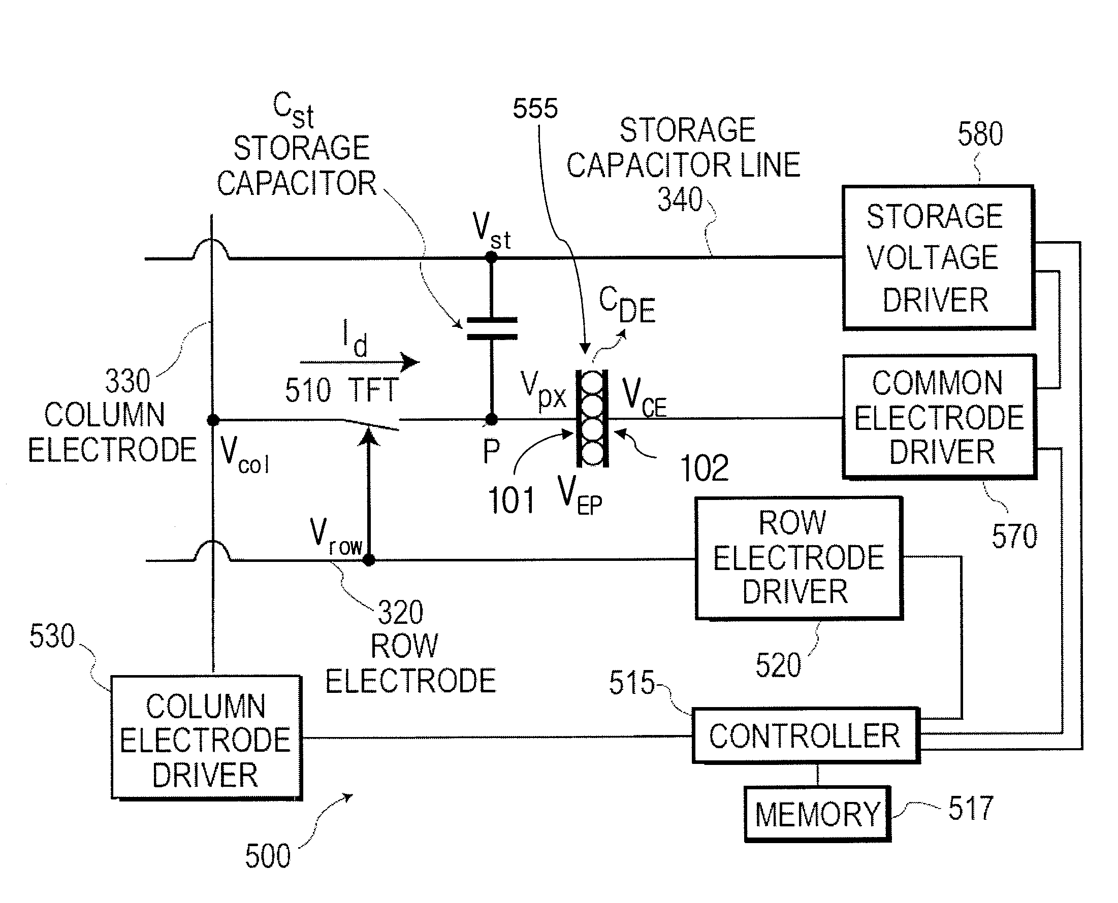
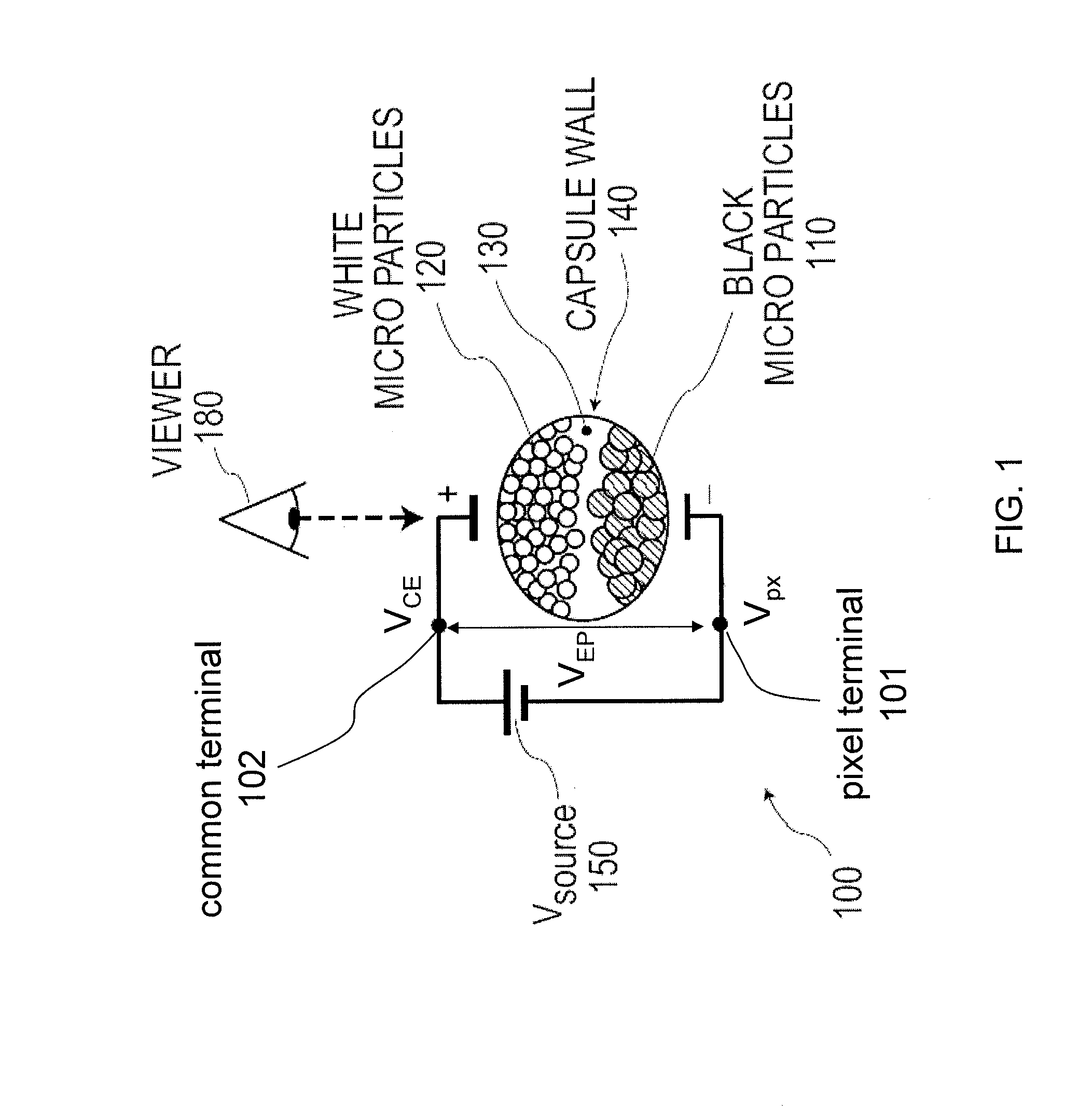
[0049]The following description of certain exemplary embodiments is merely exemplary in nature and is in no way intended to limit the invention, its application, or uses. In the following detailed description of embodiments of the present systems, devices and methods, reference is made to the accompanying drawings which form a part hereof, and in which are shown by way of illustration specific embodiments in which the described devices and methods may be practiced. These embodiments are described in sufficient detail to enable those skilled in the art to practice the presently disclosed systems and methods, and it is to be understood that other embodiments may be utilized and that structural and logical changes may be made without departing from the spirit and scope of the present system.

[0050]The following detailed description is therefore not to be taken in a limiting sense, and the scope of the present system is defined only by the appended claims. The leading digit(s) of the ref...


PUM


Abstract

A display device (500) is described with a plurality of pixels (555), each having a pixel state (P) that is driven by a driving voltage differential (VEP) between a pixel voltage (Vpx) applied to a pixel terminal (101) of the pixel and a common voltage (VCE) applied to a common terminal (102) of the pixel. In a first pixel driving state, wherein pixels are driven to a first colour, a common voltage is provided to the common terminals (102) with a first polarity. In a second pixel driving state, wherein pixels are driven to a second colour, a common voltage is provided to the common terminals (102) with a second polarity opposite to the first polarity. An absolute value of the common voltage (VCE) in the first and second pixel driving state is higher than a maximum absolute value of the column voltage (Vcol) in the corresponding pixel driving state.

Description

FIELD AND BACKGROUND OF THE INVENTION[0001]The present invention relates to display devices, such as devices driving an active matrix electrophoretic display by varying the common voltage.[0002]Displays, such as liquid crystal (LC) and electrophoretic displays include particles suspended in a medium sandwiched between a drive or pixel terminal and a common terminal. The pixel terminal can be controlled in various ways. The most simple and low cost way is direct control of the pixel electrode by a display controller. This is called a direct-drive or segmented display, where every pixel (also called a segment in this type of display) is under the direct control of the controller. Another way to control the pixel terminal is by way of passive-matrix driving, where the pixel terminals are connected to each other in rows and the common terminals are connected to each other in columns, where each row and column are under the direct control of a display controller. This way a simple matrix...

Claims


Application Information

Patent Timeline
IPC IPC(8): G06F3/038
CPCG09G3/344G09G2300/0876G09G2310/0251G09G2310/0254G09G2320/0257G09G2330/021G09G3/3225G09G2310/0235G09G2320/0214G09G2320/0219
Inventor VAN VEENENDAAL, ERIKHUITEMA, HJALMAR EDZER AYCO
Owner SAMSUNG ELECTRONICS CO LTD
Why Eureka
Try Eureka