Memory Device, Manufacturing Method and Operating Method of the Same

a memory device and manufacturing method technology, applied in semiconductor devices, digital storage, instruments, etc., can solve the problems of difficult to overcome limitation, memory device performance may also be limited, and the scaling limitation of this kind of memory device is still bigger than 50 nm, so as to achieve small scaling feature and good performance

Active Publication Date: 2012-07-19
MACRONIX INT CO LTD
View PDF4 Cites 170 Cited by
  • Summary
  • Abstract
  • Description
  • Claims
  • Application Information

AI Technical Summary

Benefits of technology

[0006]The disclosure is directed to a memory device, a manufacturing method and an operati

Problems solved by technology

However, the scaling limitation of a memory cell size of this kind of the memory device is still bigger than 50 nm.
It is no

Method used


Image

  • Memory Device, Manufacturing Method and Operating Method of the Same
  • Memory Device, Manufacturing Method and Operating Method of the Same
  • Memory Device, Manufacturing Method and Operating Method of the Same

Examples


Embodiment Construction

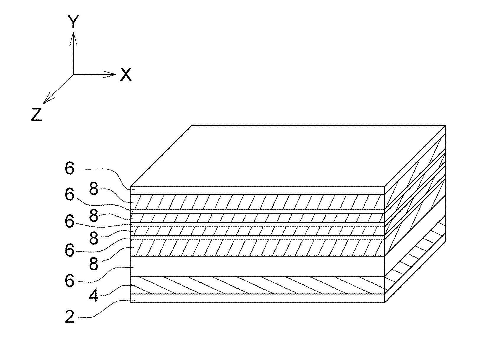
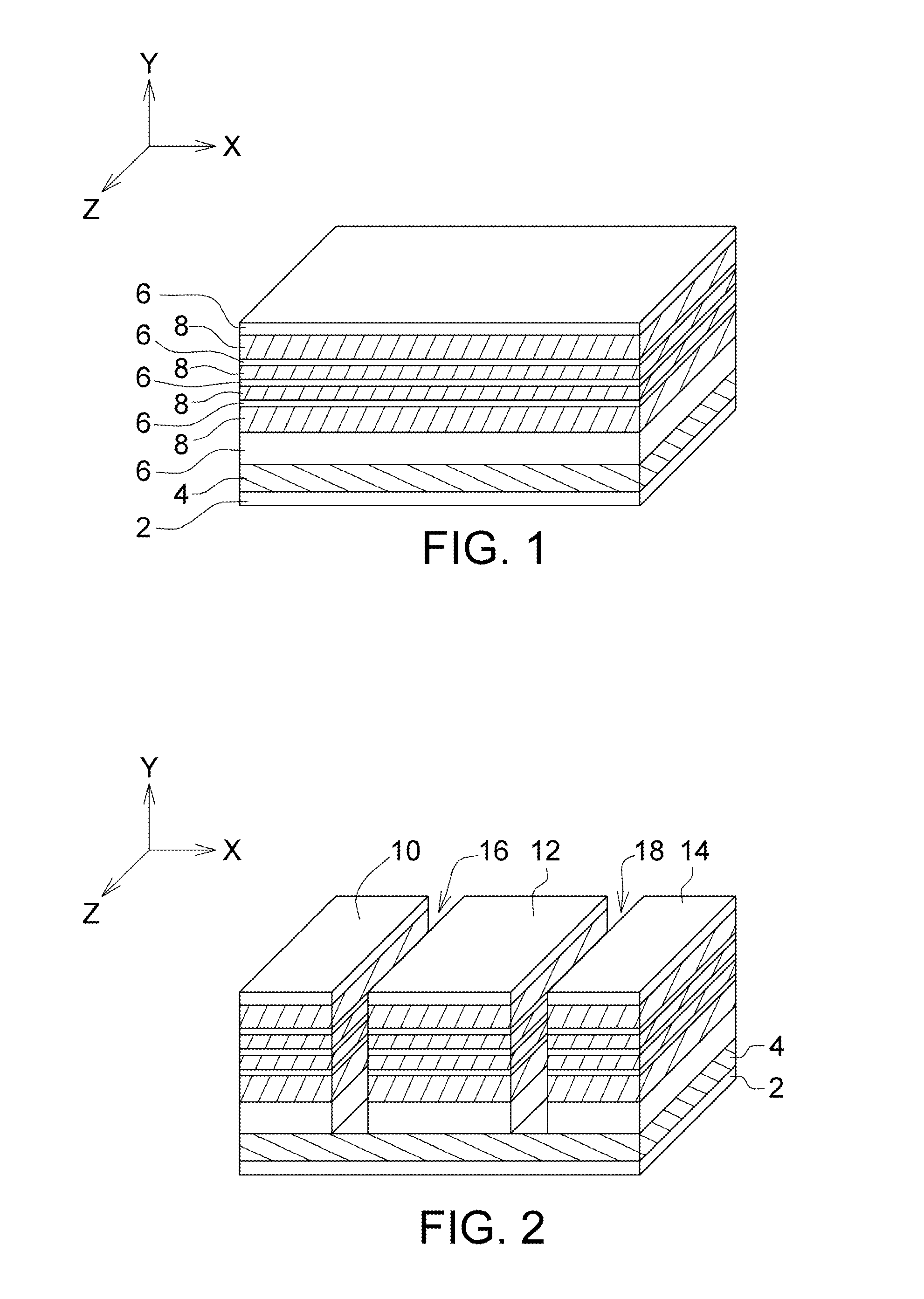
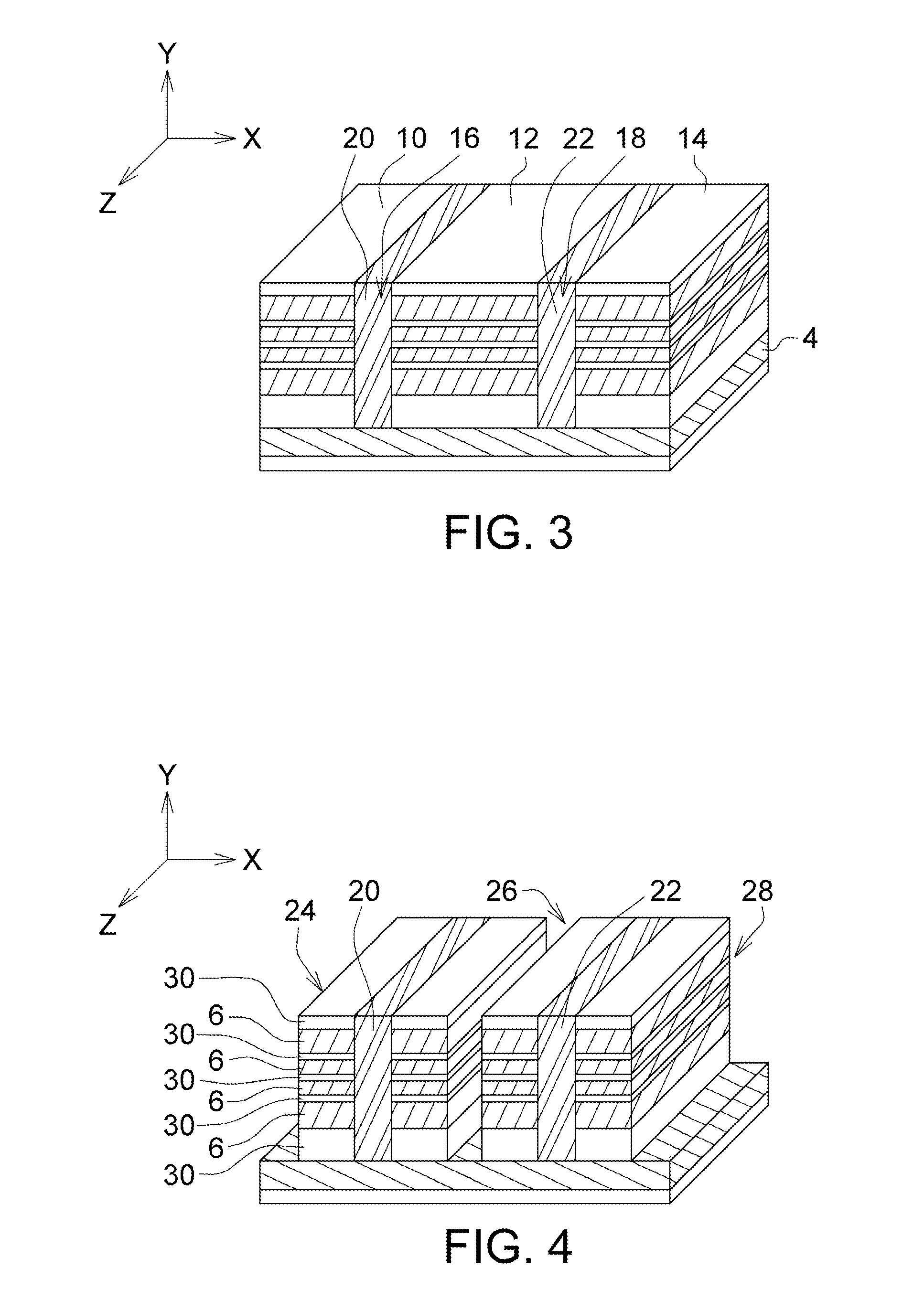
[0019]FIGS. 1-13 illustrate a method for manufacturing a memory device in one embodiment. Referring to FIG. 1, a source element 4 is disposed on a substrate 2. In embodiments, the source element 4 may comprise a source layer or a source line. The embodiment as shown in FIGS. 1-13 is illustrated by using the source element 4 being the source layer covering the substrate 2. The source element 4 may have N+ type conductivity. In one embodiment, the source element 4 is disposed on and insulated from the substrate 2. For example, the source element 4 and the substrate 2 are separated from each other by a dielectric structure (not shown). Sacrificial layers 6 and insulating layers 8 are alternately stacked on the source element 4. The sacrificial layers 6 are separated from each other by the insulating layers 8. The sacrificial layer 6 may comprises a nitride such as silicon nitride. The insulating layer 8 may comprise an oxide such as silicon oxide. The most bottom one of the insulating ...


PUM


Abstract

A memory device, a manufacturing method and an operating method of the same are provided. The memory device includes a substrate, stacked structures, a channel element, a dielectric element, a source element, and a bit line. The stacked structures are disposed on the substrate. Each of the stacked structures includes a string selection line, a word line, a ground selection line and an insulating line. The string selection line, the word line and the ground selection line are separated from each other by the insulating line. The channel element is disposed between the stacked structures. The dielectric element is disposed between the channel element and the stacked structure. The source element is disposed between the upper surface of the substrate and the lower surface of the channel element. The bit line is disposed on the upper surface of the channel element.

Description

BACKGROUND[0001]1. Technical Field[0002]The disclosure relates in general to a memory device, a manufacturing method and an operating method of the same and more particularly to a 3D vertical gate memory device, a manufacturing method and an operating method of the same.[0003]2. Description of the Related Art[0004]Memory devices are used in storage elements for many products such as MP3 players, digital cameras, computer files, etc. As the application increases, the demand for the memory device focuses on small size and large memory capacity. For satisfying the requirement, a memory having a high element density is need.[0005]Designers have developed a method for improving a memory device density, using 3D stack memory device so as to increase a memory capacity and a cost per cell. However, the scaling limitation of a memory cell size of this kind of the memory device is still bigger than 50 nm. It is not easy to breakthrough the limitation. The performance of the memory device may ...

Claims


Application Information

Patent Timeline
IPC IPC(8): G11C16/04H01L29/792H01L21/336
CPCG11C16/0466G11C16/3418H01L29/66833H01L27/11582H01L29/7926H01L27/11578H10B43/20H10B43/27
Inventor LUE, HANG-TINGCHEN, SHIH-HUNG
Owner MACRONIX INT CO LTD
Why Eureka
Try Eureka