
Gallium-Nitride-on-Handle Substrate Materials and Devices and Method of Manufacture

a technology of gallium nitride and substrate, which is applied in the direction of basic electric elements, electrical apparatus, and semiconductor devices, can solve the problems of low thermal conductivity, significant mismatch in thermal expansion coefficient with respect to gan layer, and not being aware of the best way to arrange fabricated devices with respect, etc., to achieve high quality and ease of implementation

Inactive Publication Date: 2012-07-26
SLT TECH
View PDF3 Cites 111 Cited by
  • Summary
  • Abstract
  • Description
  • Claims
  • Application Information

AI Technical Summary

Benefits of technology

[0012]The present device and method provides for an improved gallium and nitrogen containing material and resulting device structures for optical and electronic devices. In other embodiments, the present method and resulting structure are easier to implement using conventional technologies. The invention provides a high quality GaN substrate and resulting devices. These and other benefits are further described below in conjunction with the attached drawings.

Problems solved by technology

Sapphire, while readily available and convenient to work with, suffers from a relatively low thermal conductivity and has a significant mismatch in the coefficient of thermal expansion with respect to the GaN layer.
In addition, in cases where the nitride crystal in a GaN-on-insulator wafer is spatially inhomogeneous, we are not aware of any teachings about the best way to arrange fabricated devices with respect to structures in the GaN layer.

Method used


Image

  • Gallium-Nitride-on-Handle Substrate Materials and Devices and Method of Manufacture
  • Gallium-Nitride-on-Handle Substrate Materials and Devices and Method of Manufacture
  • Gallium-Nitride-on-Handle Substrate Materials and Devices and Method of Manufacture

Examples


Embodiment Construction

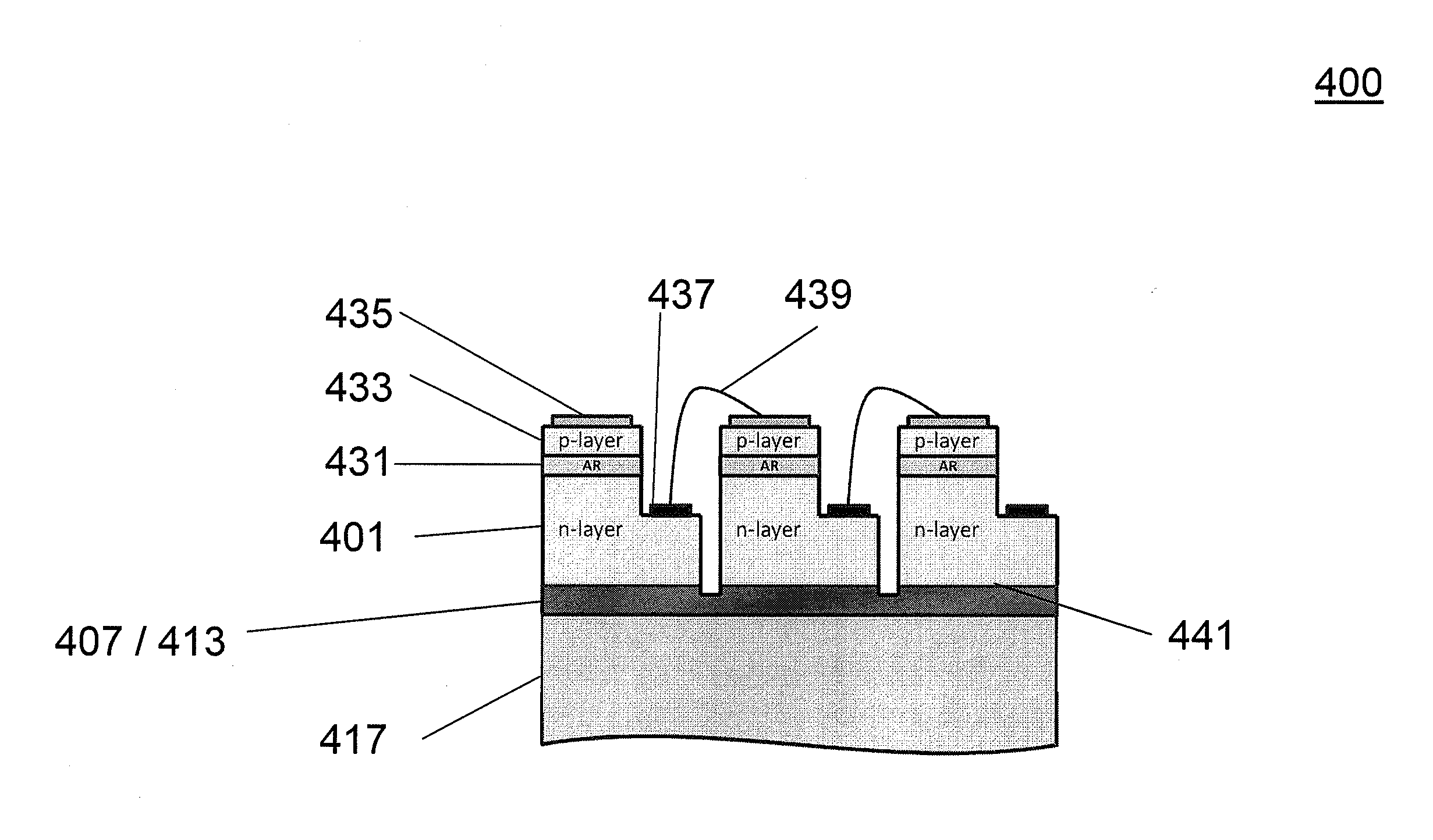
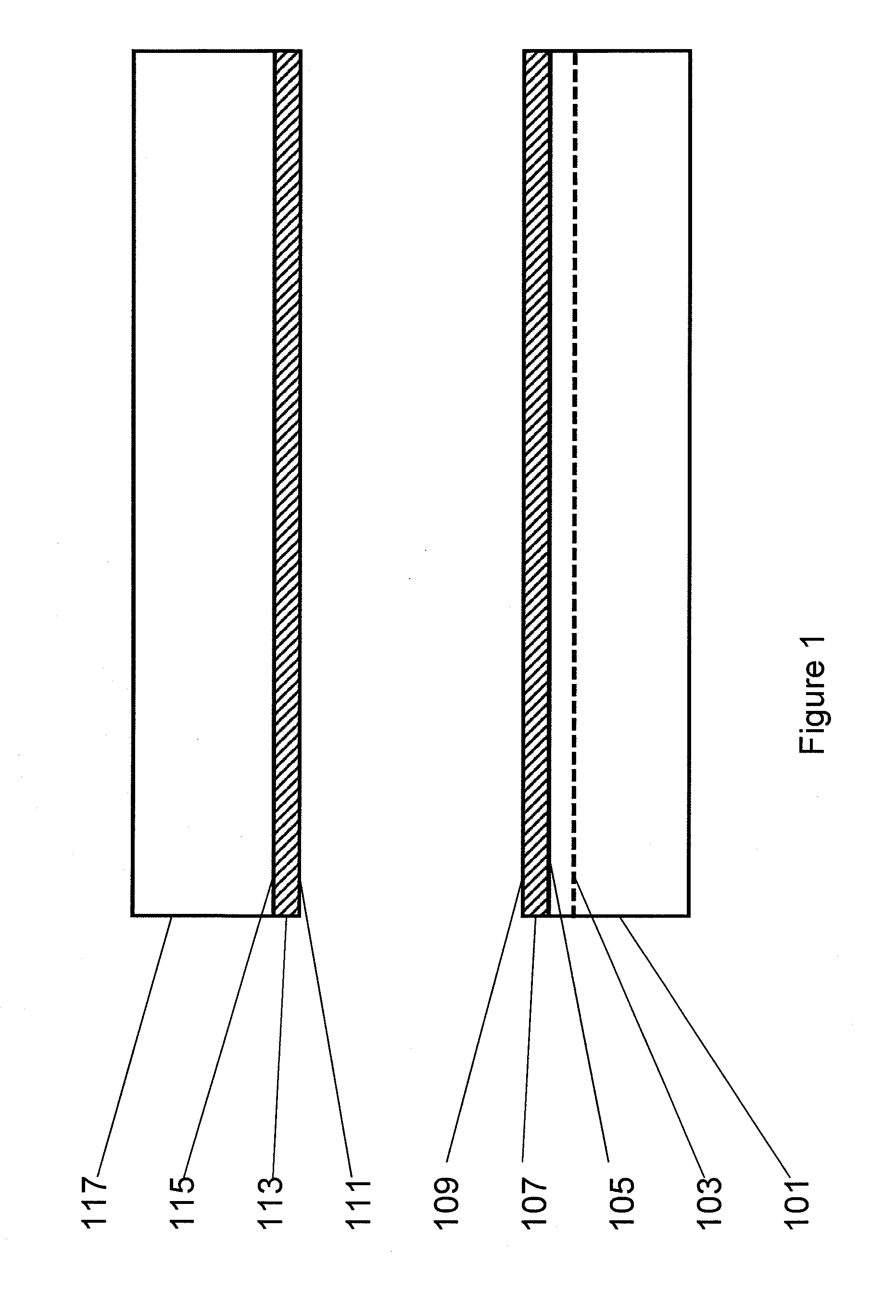
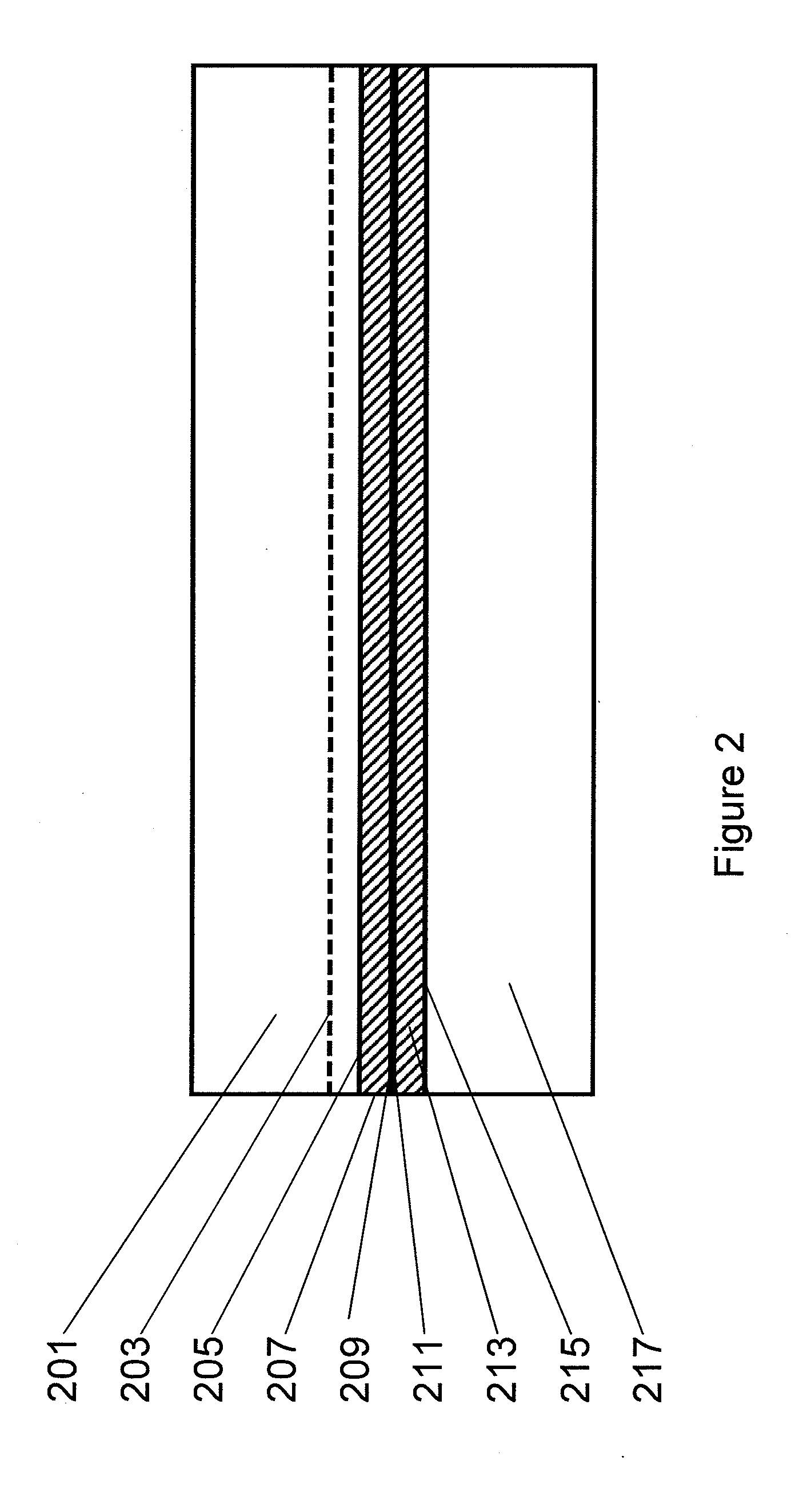
[0034]Referring to FIG. 1, in one set of embodiments the starting point for the present invention is a donor substrate 101 consisting essentially of a high quality nitride crystal or wafer.

[0035]The nitride crystal comprises nitrogen and has a threading dislocation density below about 108 cm−2. The nitride crystal or wafer may comprise AlxInyGa1-x-yN, where 0≦x, y, x+y≦1, for example, GaN. In a preferred embodiment, the nitride crystal is substantially free of low-angle grain boundaries, or tilt boundaries, over a length scale of at least 3 millimeters.

[0036]The nitride crystal or wafer may have a large-surface orientation within ten degrees, within five degrees, within two degrees, within one degree, within 0.5 degree, or within 0.2 degree of (0 0 0 1), (0 0 0 −1), {1 −1 0 0}, {1 1 −2 0}, {1 −1 0 ±1}, {1 −1 0 ±2}, {1 −1 0 ±3}, {2 0 −2 ±1}, or {1 1 −2 ±2}. In one specific embodiment, the nitride crystal has a semipolar large-surface orientation, which may be designated by (hkil) Bra...


PUM


Abstract

A gallium and nitrogen containing substrate structure includes a handle substrate member having a first surface and a second surface and a transferred thickness of gallium and nitrogen material. The structure has a gallium and nitrogen containing active region grown overlying the transferred thickness and a recessed region formed within a portion of the handle substrate member. The substrate structure has a conductive material formed within the recessed region configured to transfer thermal energy from at least the transferred thickness of gallium and nitrogen material.

Description

BACKGROUND OF THE INVENTION[0001]This invention generally relates to manufacture of materials and devices. More particularly, the present invention provides a method and device using wafer-bonded crystals or the like in combination with optical devices composed of a gallium-containing nitride crystal. More specifically, embodiments of the invention include techniques for fabricating a light emitting diode device using bulk gallium nitride containing materials, for example for application to optoelectronic devices. In other embodiments, the invention provides a method of manufacture using an epitaxial gallium containing crystal with a release layer. Such crystals and materials include GaN, AN, InN, InGaN, AlGaN, and AlInGaN, and others, for manufacture of bulk or patterned substrates.[0002]Progress has been made during the past decade and a half in the performance of gallium nitride (GaN) based light emitting diodes (LEDs). Devices with a luminous efficiency higher than 100 lumens pe...

Claims


Application Information

Patent Timeline
Patent Type & Authority Applications(United States)
IPC IPC(8): H01L29/20
CPCH01L29/02H01L29/0692H01L2924/1305H01L2924/13062H01L2924/1301H01L33/50H01L33/22H01L2224/49107H01L2224/48137H01L29/2003H01L33/007H01L33/0079H01L33/32H01L33/382H01L21/6835H01L21/76254H01L2221/68327H01L2221/6835H01L2221/68381H01L2224/48091H01L2924/00014H01L2924/00H01L2924/12032H01L24/29H01L24/83H01L2224/73265H01L2224/83193H01L2924/12042H01L2924/12041H01L2924/12043H01L33/0093
Inventor D'EVELYN, MARK P.CHAKRABORTY, ARPANHOUCK, WILLIAM
Owner SLT TECH
Features
  • Generate Ideas
  • Intellectual Property
  • Life Sciences
  • Materials
  • Tech Scout
  • Unparalleled Data Quality
  • Higher Quality Content
  • 60% Fewer Hallucinations
Learn More