Method for packaging wafer

a technology of wafers and packaging, applied in the direction of basic electric elements, electrical apparatus, semiconductor devices, etc., can solve the problems of difficulty in forming through silicon vias, insulation problems of through silicon vias, and damage to existing circuitry, so as to reduce the cost of substrate, reduce the cost of wire bonding and molding/encapsulation process, and achieve high density chips.

Inactive Publication Date: 2012-07-26
TU JIA JIN +1
View PDF5 Cites 1 Cited by
  • Summary
  • Abstract
  • Description
  • Claims
  • Application Information

AI Technical Summary

Benefits of technology

[0008]In the present invention, the cost for the substrate, the wire bonding, and molding/encapsulating process can be reduced. Because the second chip is very thin, the connection members are provided on both the upper and lower surfaces of the chip so that the chips can be stacked on top of each other and electrically coupled to each other without i

Problems solved by technology

Because the wafer has the circuitry formed thereon, it is difficult to form the through silicon vias due to the obstruction of the circuit.
Furthermore, even if the through silicon vias can be formed, the existing circuitry may still be damaged during the electroplating or vacuum d

Method used


Image

  • Method for packaging wafer
  • Method for packaging wafer
  • Method for packaging wafer

Examples


Embodiment Construction

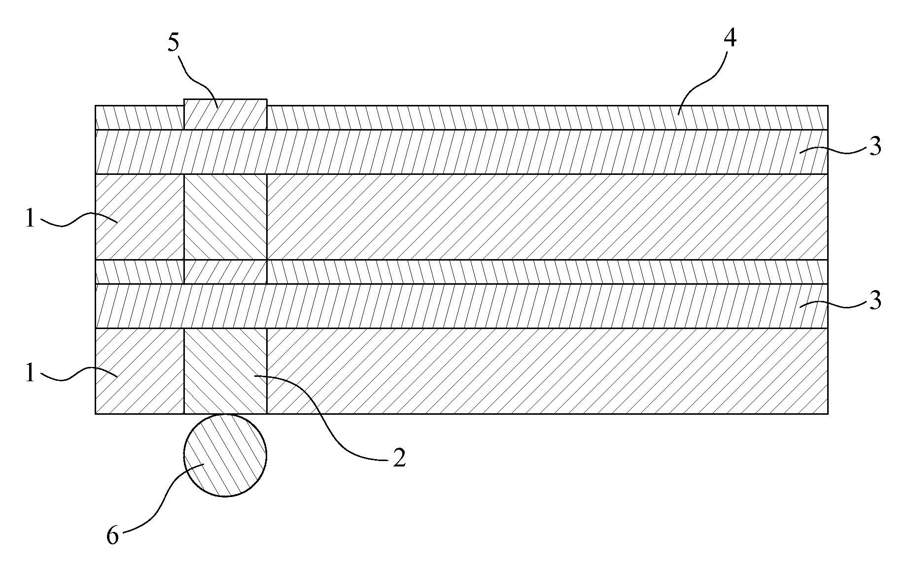
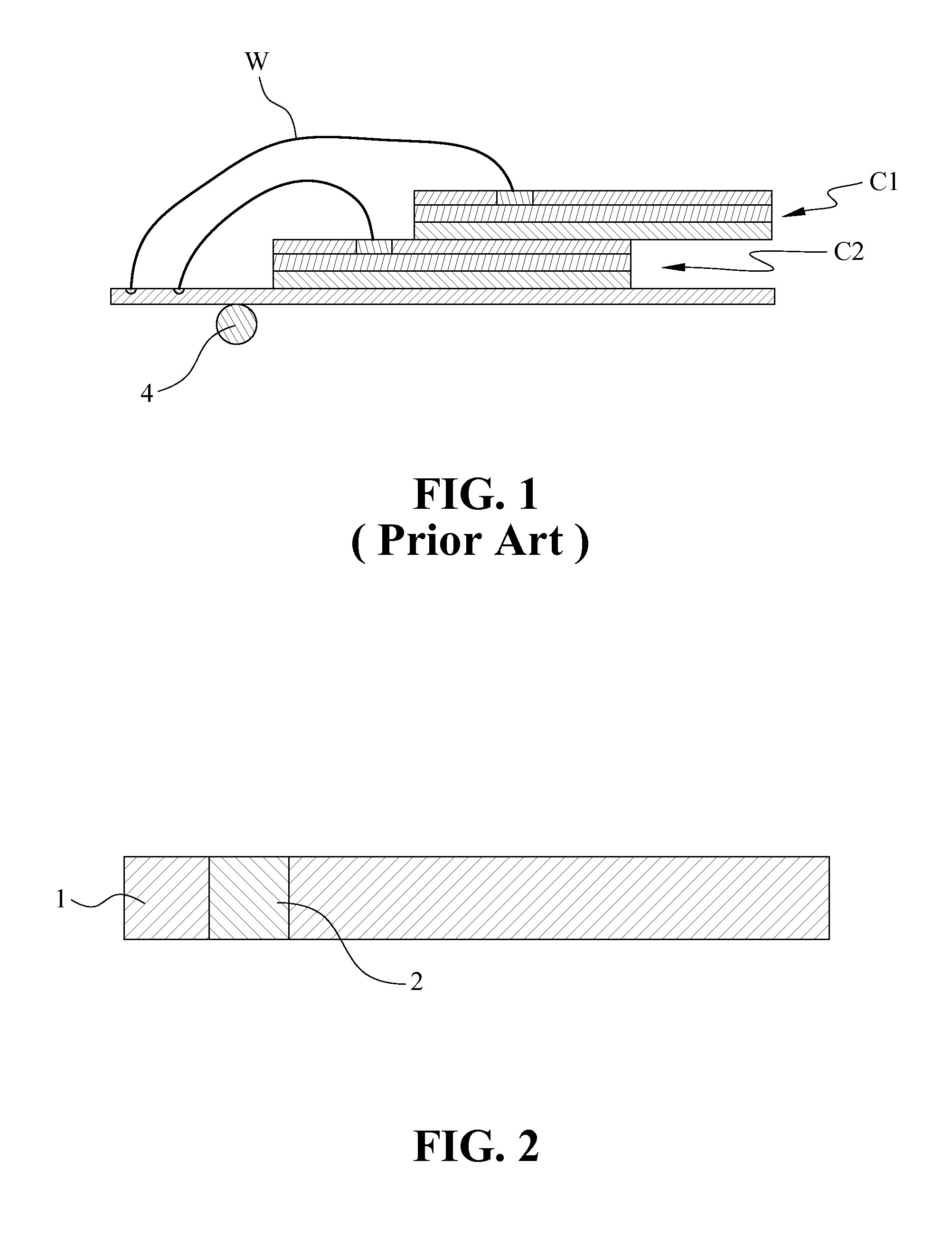
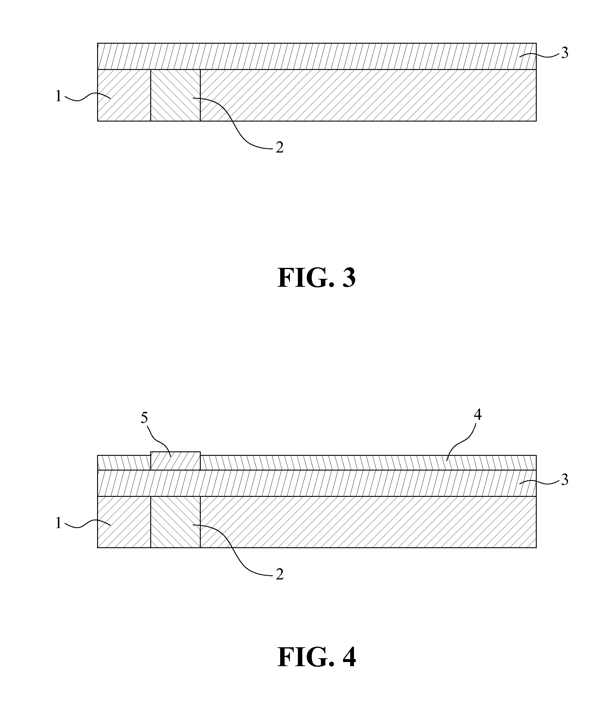
[0013]The method for packaging a wafer of the present invention comprises the steps as following: (1) a plurality of through silicon vias across through the bare wafer 1 are formed at the predetermined positions of the bare wafer 1, and the through silicon vias are filled with the conducting metal 2 (as shown in FIG. 2); (2) a redistribution layer is formed on the bare wafer 1, and the redistribution layer is connected to each of the through silicon vias; (3) a chemical mechanical polishing process is performed to planarize a surface of the bare wafer 1; (4) a wafer forming process is performed to treat the planarized bare wafer; (5) a metal layer 3 is formed on the wafer 1 after processed (as shown in FIG. 3); (6) a plurality of connection pads 5 are formed on the metal layer 3, and the connection pads 5 are respectively electrically connected to their corresponding through silicon vias (as shown in FIG. 4); (7) a passivation layer 4 is formed on the metal layer 3 (referring to FIG...


PUM


Abstract

A method for packaging a wafer is provided, which includes: providing a bare wafer; forming a plurality of through silicon vias across through the bare wafer, the through silicon vias being filled with a conducting metal; forming a redistribution layer on the bare wafer, the redistribution layer being connected to each of the through silicon vias; performing a chemical mechanical polishing process to planarize a surface of the bare wafer; performing a wafer forming process to treat the planarized bare wafer; forming a metal layer on the wafer after processed; forming a plurality of connection pads on the metal layer, the connection pads being respectively electrically connected to their corresponding through silicon vias; forming a passivation layer on the metal layer; and forming a plurality of solder balls or metal bumps on a backside surface of the wafer through which the processed wafer is electrically connected to a substrate.

Description

BACKGROUND OF THE INVENTION[0001]1. Field of the Invention[0002]The present invention relates to a method for packaging a wafer, and more particularly to a method for packaging a wafer in which the through silicon vias (TSV) and the redistribution layer (RDL) are formed on a bare wafer before the semiconductor circuits are formed thereon.[0003]2. The Prior Arts[0004]In a conventional method for packaging a wafer level package, the wafer is packaged after the circuits have been formed thereon. Because the wafer has the circuitry formed thereon, it is difficult to form the through silicon vias due to the obstruction of the circuit. Furthermore, even if the through silicon vias can be formed, the existing circuitry may still be damaged during the electroplating or vacuum deposition process applied for filling the through silicon vias. Because the formation of the circuitry on the wafer is completed, the insulation problem for the through silicon vias may exist. Furthermore, the surface...

Claims


Application Information

Patent Timeline
IPC IPC(8): H01L21/78
CPCH01L2224/48091H01L2224/48227H01L2924/00014H01L2224/04042H01L2224/0401H01L2924/3025H01L2924/10253H01L2224/05025H01L2224/05008H01L2224/02372H01L2224/02317H01L25/0657H01L24/94H01L24/13H01L24/05H01L2224/93H01L2224/05569H01L2225/06565H01L2225/06541H01L2225/06562H01L2924/15311H01L21/76898H01L2224/0557H01L2224/13025H01L2224/131H01L2225/06517H01L2225/06513H01L2924/014H01L2224/11H01L2924/00015H01L2924/00H01L2224/05552
Inventor TU, JIA-JINLEE, YING-HUANG
Owner TU JIA JIN
Why Eureka
Try Eureka