Method for recycling a source substrate

a source substrate and recycling technology, applied in the direction of semiconductor devices, semiconductor/solid-state device details, electrical equipment, etc., can solve the problems of long and costly chemical-mechanical polishing procedures, no completely satisfactory methods, and the material of certain source substrates (sic, gan, aln, etc.) is relatively hard and difficult to polish, so as to facilitate selective removal of such regions and facilitate recycling of source substrates

Inactive Publication Date: 2012-08-09
SOITEC SA
View PDF4 Cites 21 Cited by
  • Summary
  • Abstract
  • Description
  • Claims
  • Application Information

AI Technical Summary

Benefits of technology

[0019]The present invention aims to make removal of the ring of residual material on a donor substrate easier and therefore to make recycling this substrate easier, by reducing the duration, the quality and the cost of the recycling operations.

Problems solved by technology

None of these methods are completely satisfactory, however, and the materials of certain source substrates (SiC, GaN, AlN, AlGaN, etc.) are relatively hard and difficult to polish.
The chemical-mechanical polishing is therefore a long and costly procedure.
Energy-based techniques, such as those using a laser beam, are not selective to the regions of relief and may damage the rest of the source substrate unless they are controlled very precisely.
In addition, substrates have increasingly large diameters (six inches for example or more), thereby amplifying the aforementioned difficulties.
In particular there is a risk that defects, for example micro-scratches, will form if excessive polishing or non-selective energy techniques are used.

Method used


Image

  • Method for recycling a source substrate
  • Method for recycling a source substrate
  • Method for recycling a source substrate

Examples


example

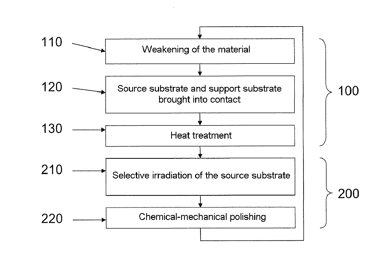
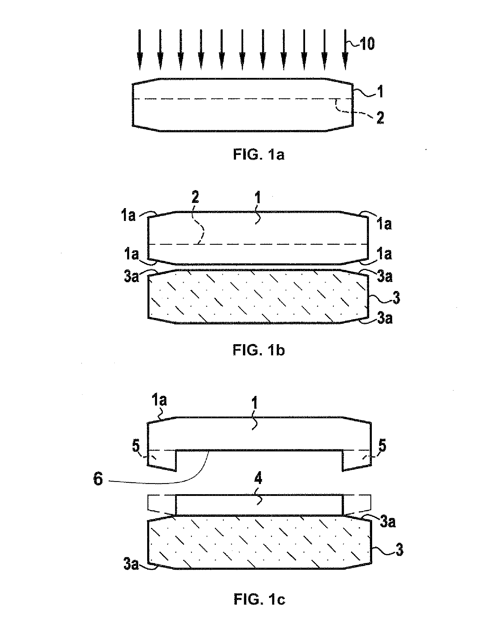
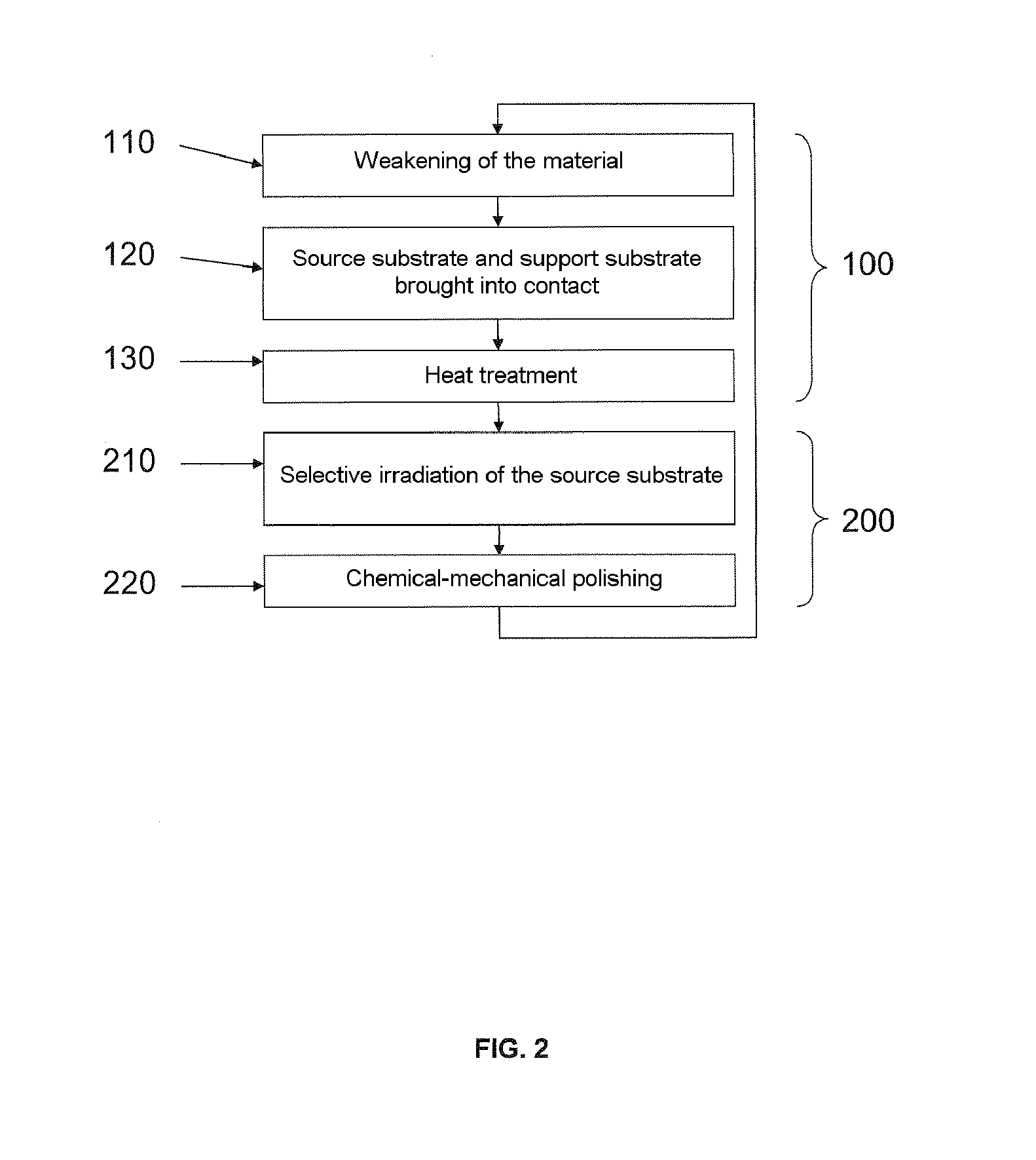
[0070]On a self-supporting GaN source substrate 1 a layer of silicon oxide 500 nm in thickness was deposited. Hydrogen with a dose higher than 1×10¹⁶ atoms / cm2 and an energy of 50 to 150 keV, depending on the thickness of the layer 4 to be transferred, was implanted into the GaN through the oxide layer. This led to an average species density of about 1×10²¹ atoms / cm3 near the weakened zone 2 and the material became absorbent at a wavelength longer than or equal to 370 nm. In addition, a layer of 500 nm of silicon oxide was deposited on a sapphire support substrate 3.

[0071]The GaN and sapphire substrates were then brought into contact so as to bond them. Their surfaces can possibly be polished just before this contacting step—it is preferable for the RMS surface roughness measured by AFM (atomic force microscope) to be less than 5 ångströms over a 5 micron×5 micron field (this field corresponding to the size of the observed zone).

[0072]RMS roughness means the root-mean-square roughne...


PUM


Abstract

The present invention relates to process for recycling a source substrate that has a surface region and regions in relief on the surface region, with the regions in relief corresponding to residual regions of a layer of the source substrate that were not being separated from the rest of the source substrate during a prior removal step. The process includes selective electromagnetic irradiation of the source substrate at a wavelength such that the damaged material of the surface region absorbs the electromagnetic irradiation. The present invention also relates to a recycled source substrate and to a process for transferring a layer from a source substrate recycled for this purpose.

Description

TECHNICAL FIELD[0001]The field of the invention is that of semiconductor substrates used in the electronics, optics or optoelectronics industry.[0002]The invention more precisely relates to the recycling of semiconductor substrates from which a thin layer of material has been removed.BACKGROUND ART[0003]Silicon-on-insulator (SOI) structures are structures consisting of a multilayer comprising a very thin layer of silicon on an insulator layer, itself generally on a substrate. These structures are increasingly used in the electronics industry because of their superior performance.[0004]This type of structure is generally produced using Smart-Cut™ technology and FIGS. 1a-c show the main steps for producing an SOI wafer.[0005]FIG. 1a shows a source or “donor” substrate 1 one side of which is subjected to implantation via bombardment with ionic species 10 (for example H+ ions) so as to create, at a certain depth in the substrate, a weakened zone 2. As illustrated in FIG. 1b, the side of...

Claims


Application Information

Patent Timeline
Patent Type & Authority Applications(United States)
IPC IPC(8): H01L29/02H01L21/762H01L21/02
CPCH01L21/76254H01L21/02032H01L27/12
Inventor LECOMTE, MONIQUEGUENARD, PASCALRIGAL, SOPHIESOTTA, DAVIDJANIN, FABIENNEVEYTIZOU, CHRISTELLE
Owner SOITEC SA
Why Eureka
Try Eureka