Self-healing analog-to-digital converters with background calibration

a technology of analog-to-digital converters and background calibration, which is applied in the direction of code conversion, transmission systems, instruments, etc., can solve the problems of reducing the linearity of adc, affecting the overall performance of adc, and high hardware overhead, so as to reduce the extra area and power overhead, not to degrade the overall performance.

Active Publication Date: 2012-08-16
UNIV OF FLORIDA RES FOUNDATION INC
View PDF7 Cites 23 Cited by
  • Summary
  • Abstract
  • Description
  • Claims
  • Application Information

AI Technical Summary

Benefits of technology

[0009]According to one aspect of an embodiment of the invention, a calibration method is provided that incurs minimal extra area and power overhead.
[0010]According to another asp

Problems solved by technology

However, small transistors tend to lead to larger offsets in the comparators, which degrade the linearity of the ADC.
High hardware overhead may exist due to captive loa

Method used


Image

  • Self-healing analog-to-digital converters with background calibration
  • Self-healing analog-to-digital converters with background calibration
  • Self-healing analog-to-digital converters with background calibration

Examples


example

5-Bit ADC with Background Calibration

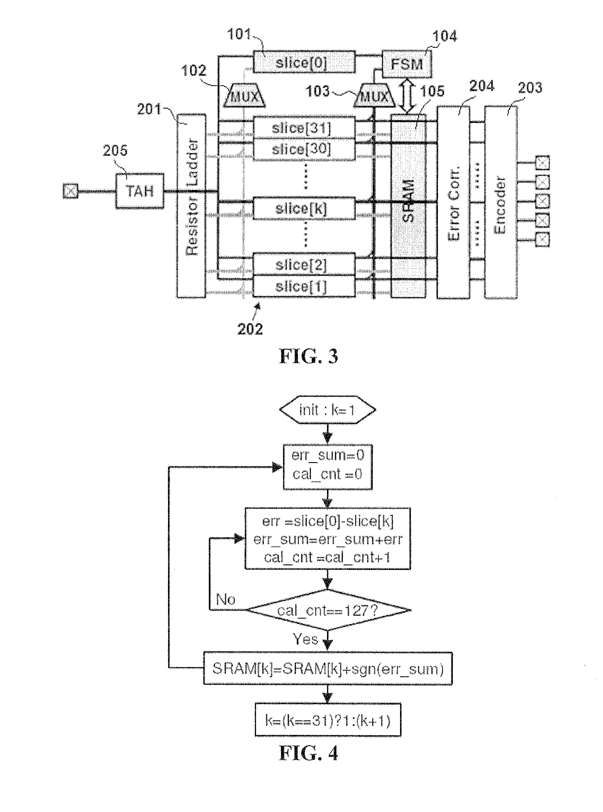
[0061]A self-healing 5-hit ADC according to an embodiment of the invention was designed as shown in the simplified schematic of FIG. 5. A test chip was implemented in 0.13 μm hulk CMOS and mounted on a QFN package. FIG. 6 shows the die micrograph. The ADC occupies an active area of 0.24 mm2, of which only 2.5% is taken by the FSM and 7% by the SRAM.

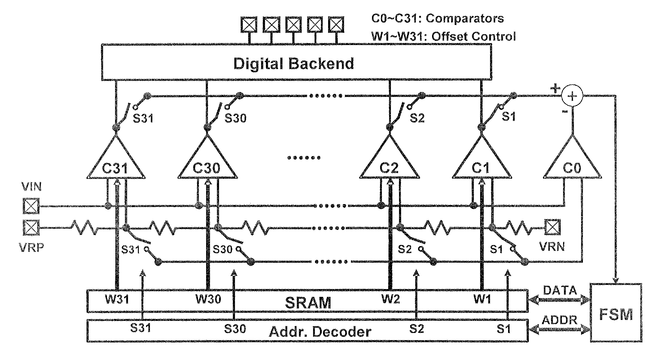
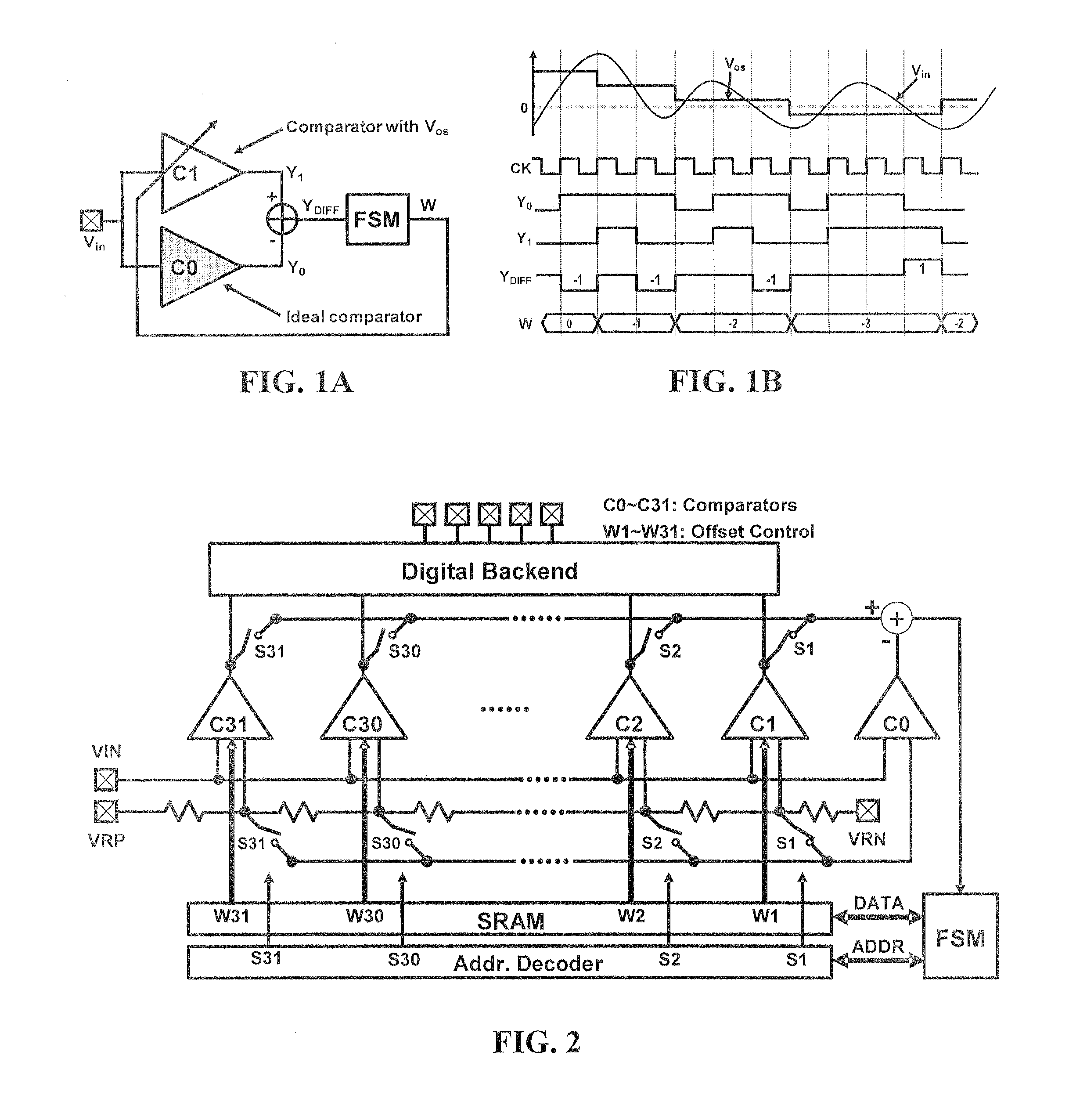
[0062]As shown in the schematic of FIG. 5, 31 comparators (comparator[1:31]) are used for digitizing an input signal and an additional reference comparator (comparator[0]) is employed. for the calibration. In the schematic, single-ended signaling is shown for simplicity; however, actual implementation is differential. The 31 comparators digitize the sampled signal against 31 evenly spaced reference voltages VREF[1:31] generated by a resistor ladder and produce a 31-bit thermometer code. The thermometer code is then converted to binary format by the digital backend. For example, the thermometer code fir...


PUM


Abstract

Calibration of an analog-to-digital converter (ADC) is accomplished via a reference comparator, a first and second multiplexer (MUX), and a finite state machine (FSM). By sampling an analog input with the reference comparator and comparing the results with those of the ADC using the FSM, all the comparators in the ADC can be calibrated without interrupting the ADC's normal operation. The first MUX provides a same reference voltage to the reference comparator as a comparator selected for the calibration, and the second MUX provides the FSM with the output of the selected comparator. The FSM then performs a comparison of the reference comparator and the selected comparator, extracts the polarity of the mismatch, and updates the contents of a memory with the extracted polarity. An offset control in the selected comparator receives a signal corresponding to the extracted polarity stored in the memory and injects offset current into the comparator.

Description

BACKGROUND OF THE INVENTION[0001]In many applications, analog signals are processed in the analog domain, converted to digital, and then further processed in the digital domain. An analog front-end is a device (in the form of an integrated circuit (IC), separate chip, or stand alone package) that receives an analog signal and performs the analog-to-digital (A / D) conversion. The analog front-end often includes signal conditioning circuits as well.[0002]Because of the continued scaling of CMOS technology, sampling of high speed signals directly at the analog front-end using analog-to-digital converters (ADCs) has been made possible. ADCs convert an analog input signal into a digital output signal by sampling the analog input signal at a sample rate and providing a digital representation of each sample to a specific resolution.[0003]Once the high speed signals are sampled using the ADCs, subsequent signal processing such as equalization and timing recovery can then be accomplished in t...

Claims


Application Information

Patent Timeline
IPC IPC(8): H03M1/00H03M1/36H03M1/10
CPCH03M1/1004H03M1/365H03M1/1061
Inventor BASHIRULLAH, RIZWANCHEN, JIKAI
Owner UNIV OF FLORIDA RES FOUNDATION INC
Why Eureka
Try Eureka