Optical backplane interconnection system and communication device

a backplane and optical technology, applied in the direction of orthogonal pcbs mounting, optical elements, instruments, etc., can solve the problems of reducing signal transmission quality, increasing the difficulty of large-capacity electrical interconnection system implementation, and reducing optical signal loss, so as to shorten the optical link, improve the transmission quality of optical signals, and reduce the loss of optical signals

Inactive Publication Date: 2012-08-23
HUAWEI TECH CO LTD
View PDF5 Cites 15 Cited by
  • Summary
  • Abstract
  • Description
  • Claims
  • Application Information

AI Technical Summary

Benefits of technology

[0009]In the embodiments of the present invention, the front board and the rear board of a circuit board located on two sides of the backplane and are disposed to be orthogonal to each other, and the optical waveguide paths in the front board and the rear board are interconnected directly throug

Problems solved by technology

However, with the limitations such as chip technologies, processes, and heat dissipation, currently, the implementation of a large-capacity electrical interconnection system becomes more and more difficult, and optical interconnection has advantages such as low loss, low cross-talk, high density, and channel characteristic unrelated with rate, so an

Method used


Image

  • Optical backplane interconnection system and communication device
  • Optical backplane interconnection system and communication device
  • Optical backplane interconnection system and communication device

Examples


Embodiment Construction

[0021]Persons in the art may further understand features and technical content of the embodiments of the present invention with reference to detailed descriptions and accompanying drawings of the embodiments of the present invention, and the accompanying drawings are provided only for reference and illustration, instead of limiting the embodiments of the present invention.

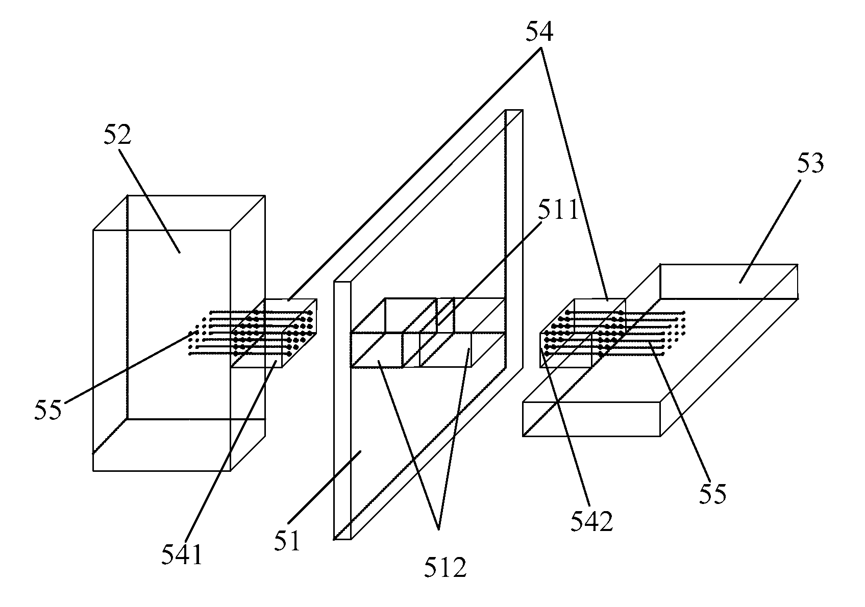
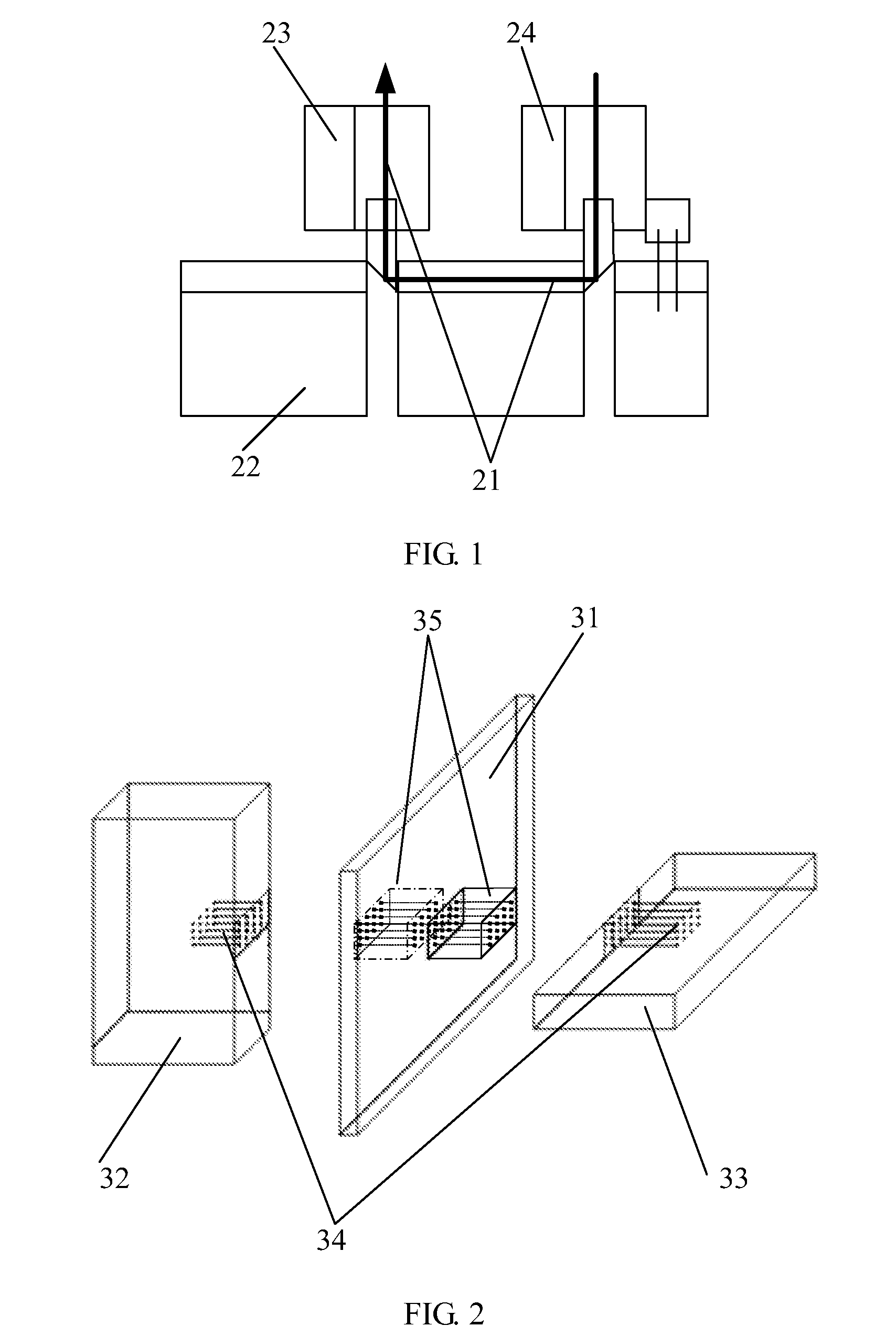
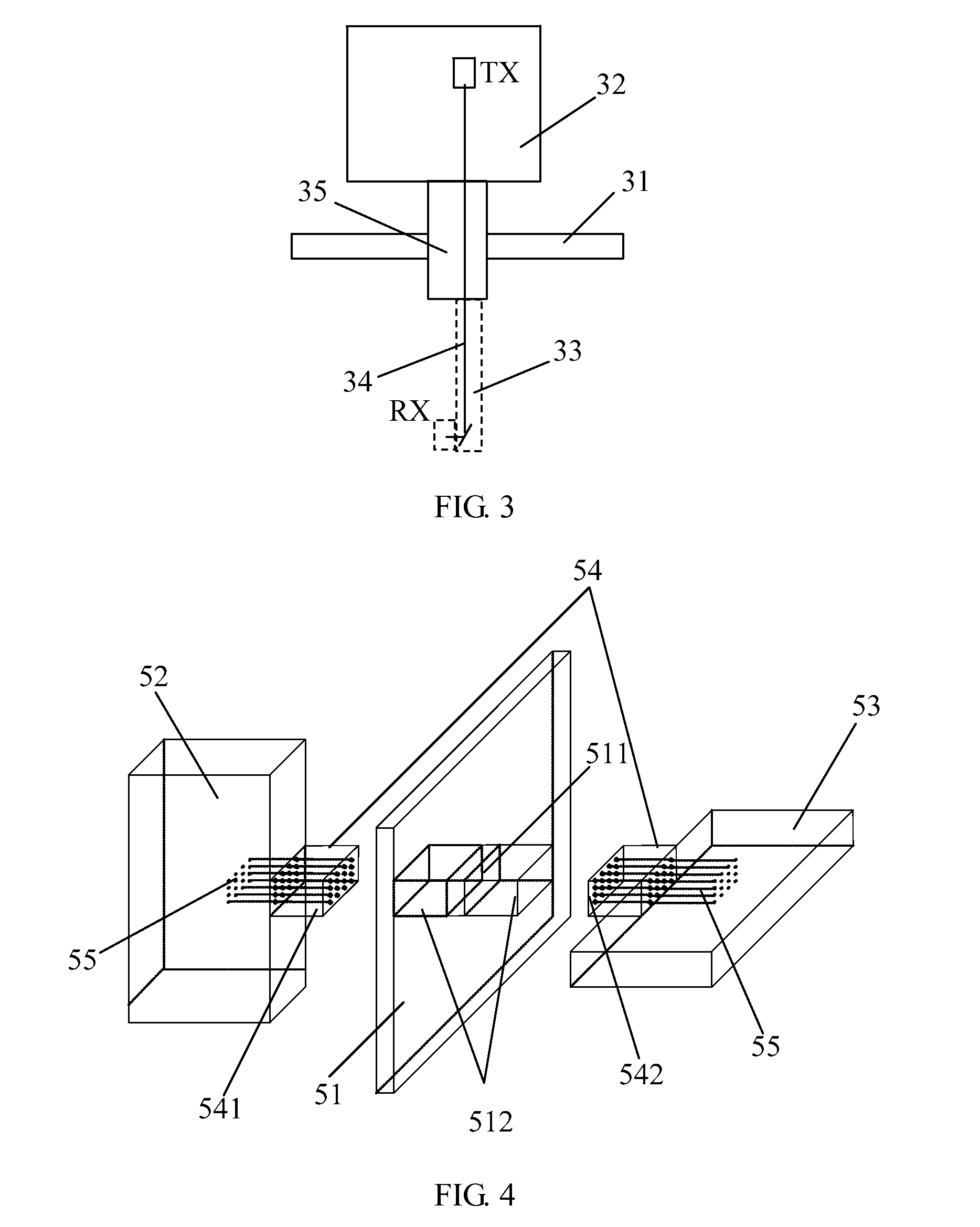
[0022]In the prior art, multi-layer polymer waveguide is obtained by performing processing of a conventional PCB (Printed Circuit Board, printed circuit board) processing technology, so that an optical backplane interconnection system has better processing performance, thereby preventing the problem of the complexity of physical implementation of a high-density fiber backplane. However, the optical waveguide itself has a large signal loss, and the optical link in the prior art is long, so that the optical signal loss is large, and the signal transmission quality is reduced. Based on this, the embodiments of the pre...


PUM


Abstract

Embodiments of the present invention provide an optical backplane interconnection system and a communication device. The optical backplane interconnection system includes a backplane, a front board, a rear board and a connector. The front board and the rear board locate on two sides of the backplane and are orthogonal to each other. The front board and the rear board are both disposed with an optical waveguide path which is interconnected through a connector connected to the backplane to form an optical path, so that optical signals can be transmitted through the optical path.

Description

CROSS-REFERENCE TO RELATED APPLICATIONS[0001]This application is a continuation of International Application No. PCT / CN2011 / 071272, filed on Feb. 24, 2011, which claims priority to Chinese Patent Application No. 201010158509.0, filed on Apr. 26, 2010, both of which are hereby incorporated by reference in their entireties.FIELD OF THE INVENTION[0002]The present invention relates to the field of communication device technologies, and in particular, to an optical backplane interconnection system and a communication device.BACKGROUND OF THE INVENTION[0003]In a communication system, access capacity of a device becomes larger and larger along with the increasing improvement of signal rate, and correspondingly, the system bandwidth is increased. Adding the number of buses is one of the manners of increasing the system bandwidth. However, with the limitations such as chip technologies, processes, and heat dissipation, currently, the implementation of a large-capacity electrical interconnect...

Claims


Application Information

Patent Timeline
IPC IPC(8): G02B6/12H04B10/80
CPCG02B6/3608G02B6/3885H05K2201/044H04B10/801H05K1/0274G02B6/43
Inventor JIA, GONGXIANLIU, WEIXIAWANG, ZEWEN
Owner HUAWEI TECH CO LTD
Why Eureka
Try Eureka