

Low-Resistance Electrode Design
- Summary
- Abstract
- Description
- Claims
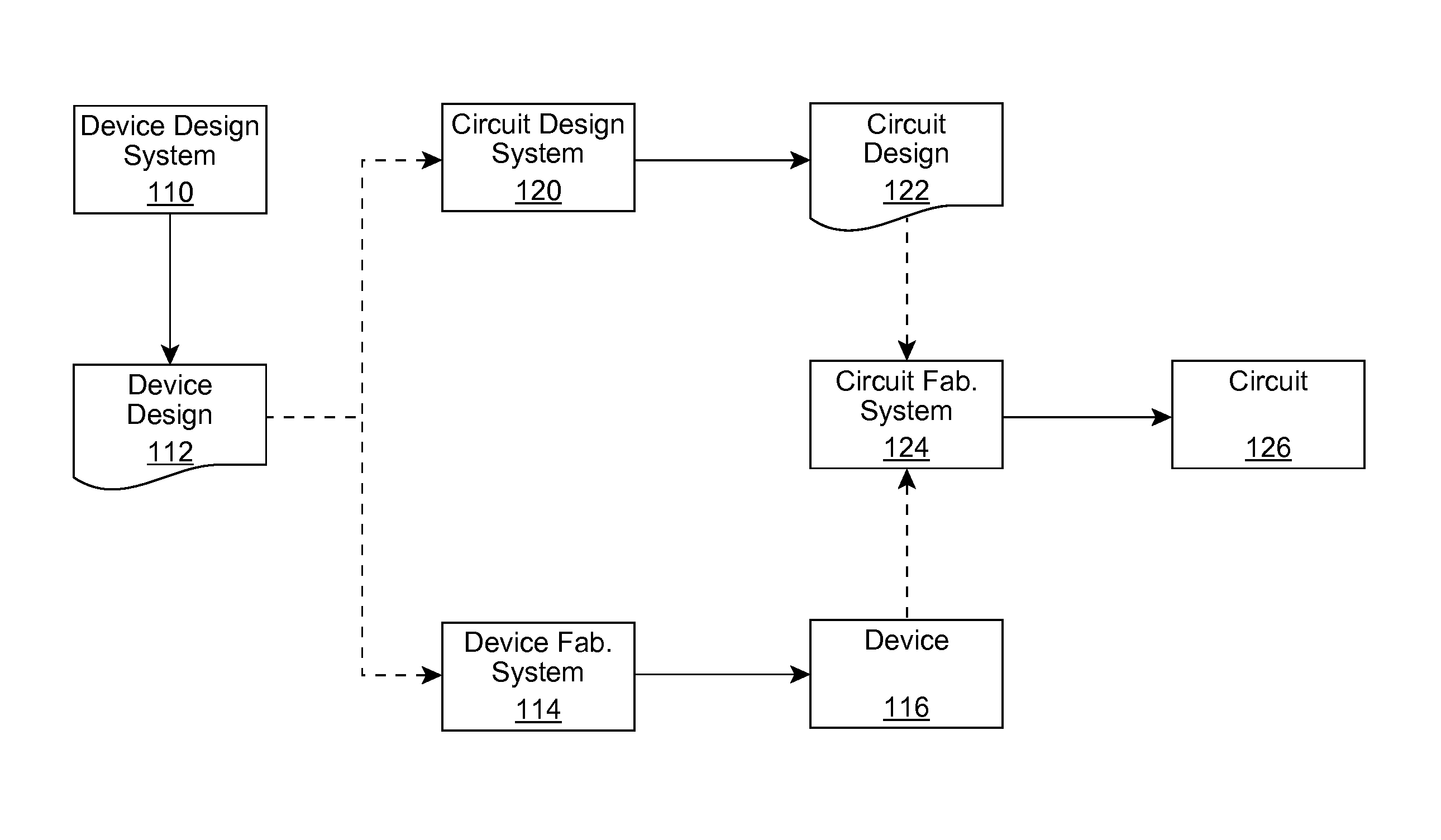
- Application Information
AI Technical Summary
Benefits of technology
Problems solved by technology
Method used
Image

Examples
Embodiment Construction
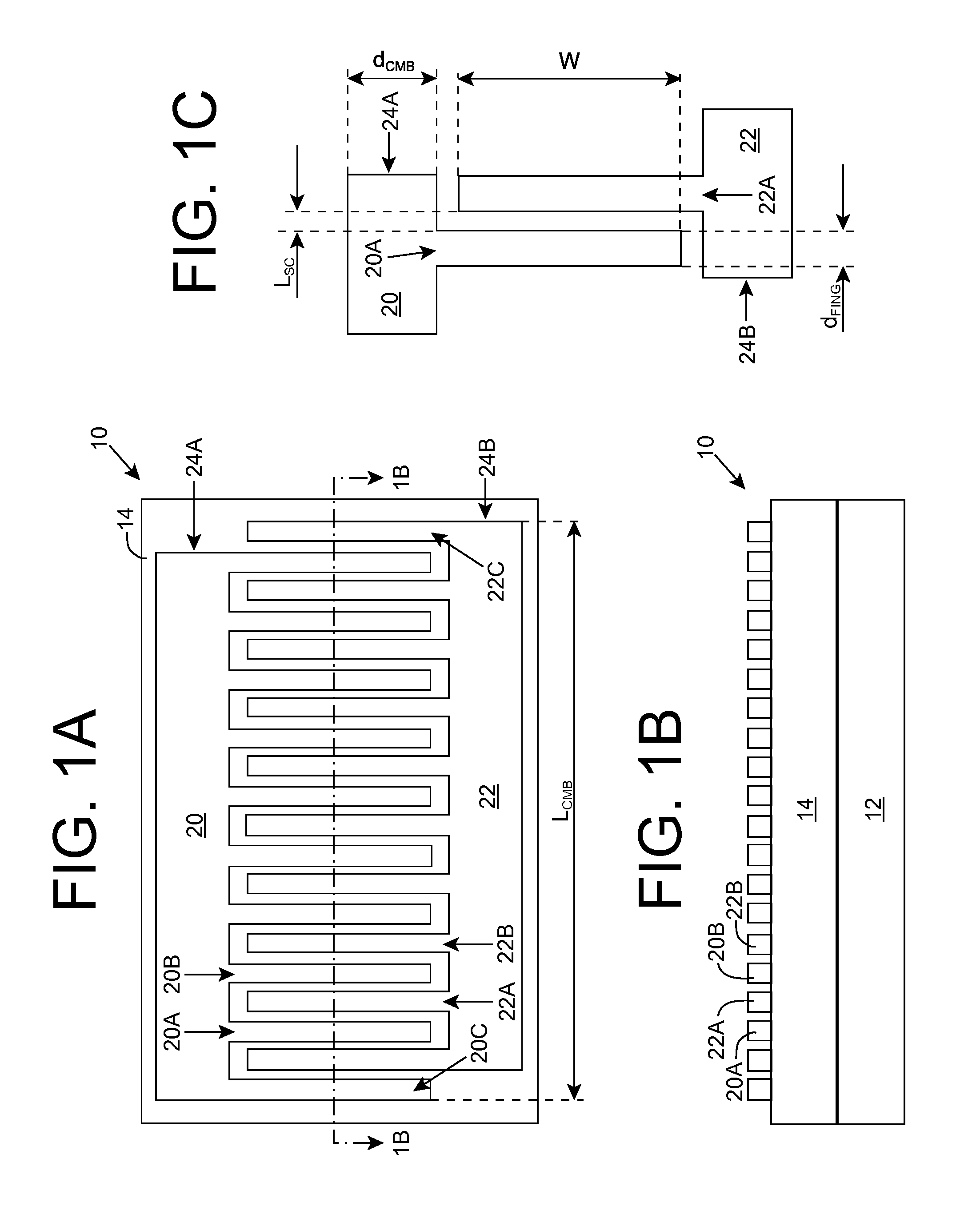
[0018]As indicated above, aspects of the invention provide a solution for designing a semiconductor device, in which two or more attributes of a pair of electrodes are determined to, for example, minimize resistance between the electrodes. Each electrode can include a current feeding contact from which multiple fingers extend, the fingers are interdigitated with the fingers of the other electrode in an alternating pattern. The attributes can include a target depth of each finger, a target effective width of each pair of adjacent fingers, and / or one or more target attributes of the current feeding contacts. Subsequently, the device and / or a circuit including the device can be fabricated. In this manner, a low total device impedance can be achieved. As used herein, unless otherwise noted, the term “set” means one or more (i.e., at least one) and the phrase “any solution” means any now known or later developed solution.
[0019]Turning to the drawings, FIGS. 1A and 1B show top and side vi...
PUM
 Abstract
Description
Claims
Application Information